

The global automotive industry is currently undergoing a paradigm shift, transitioning from traditional mechanical transport to highly sophisticated, software-defined mobility platforms. At the heart of this evolution is the rapid integration of Advanced Driver Assistance Systems (ADAS), which serve as the foundation for increasing vehicle autonomy. As manufacturers strive to enhance road safety and reduce human error, the reliance on a diverse array of sensors—including cameras, image sensors, and Light Detection and Ranging (LiDAR) components—has become absolute. However, as these sensors grow in resolution and physical size, traditional semiconductor packaging methods are reaching their physical and reliability limits. To address these emerging bottlenecks, industry experts WonBae Bang, KiDong Sim, Weilung Lu, and Adrian Arcedera have introduced a specialized Optical Ball Grid Array (OBGA) package structure designed to meet the rigorous demands of the modern automotive environment.

The Strategic Imperative for Advanced Optical Sensing
The adoption of ADAS technologies is no longer restricted to luxury vehicle segments; it has become a standard requirement for meeting global safety ratings and consumer expectations. Features such as adaptive cruise control, lane-keep assistance, and automatic emergency braking are now ubiquitous. According to the Society of Automotive Engineers (SAE) J3016 ranking system, which categorizes driving automation from Level 0 (no automation) to Level 5 (full automation), the industry is currently transitioning from Level 2 toward Levels 4 and 5.
This transition necessitates a significant increase in the number of high-resolution cameras per vehicle. While a standard vehicle might have previously utilized one or two cameras for basic rearview functions, an autonomous-capable vehicle is expected to house between 8 and 10 high-performance cameras. These optical sensors act as the "eyes" of the vehicle, providing the raw data necessary for real-time environmental interpretation. Consequently, the market for automotive image sensors is experiencing a massive boom, placing unprecedented pressure on the semiconductor supply chain to produce sensors that are not only more powerful but also more durable.

Technical Challenges in Legacy Automotive Packaging
Current packaging methodologies for automotive CMOS Image Sensors (CIS) face a critical hurdle: the Coefficient of Thermal Expansion (CTE) mismatch. Image sensors are evolving toward higher pixel counts and larger die sizes to capture more detail in diverse lighting conditions. As the sensor chip grows, the package size must increase proportionally. In a standard package, different materials—such as the silicon die, the substrate, and the protective lid—expand and contract at different rates when exposed to the extreme temperature fluctuations typical of automotive use cases.
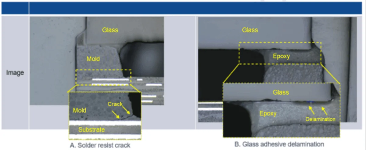
This CTE mismatch generates significant mechanical stress during thermal cycling. In legacy configurations, this stress often manifests as glass cracking, delamination of the adhesive interfaces, or internal structural failures. Furthermore, traditional packaging often utilizes metal or Liquid Crystal Polymer (LCP) lids with venting holes. While these holes manage internal pressure, they also serve as entry points for particle contamination, which can settle on the sensor area and degrade image quality—a catastrophic failure for an autonomous system relying on visual accuracy.

The industry requires a packaging solution that can scale efficiently to meet high-volume demand while providing a robust, hermetically-style seal that can survive the 15-year lifecycle of a modern vehicle.
The OBGA Solution: Architecture and Design for Manufacturing
The newly developed Optical Ball Grid Array (OBGA) package addresses these challenges by leveraging "Glass-on-Mold" (GOM) technology. This structure draws upon extensive experience in microelectromechanical systems (MEMS) and high-end consumer digital camera production. By integrating a glass lid directly onto a molded cavity, the OBGA design eliminates the need for venting holes, thereby creating a sealed environment that protects the sensitive sensor from external contaminants.

A critical component of the OBGA development process is the implementation of Design for Manufacturing (DFM) principles. The package is designed to be handled by Outsourced Semiconductor Assembly and Test (OSAT) providers, allowing for scalable, cost-effective production. The research team utilized advanced thermomechanical modeling to analyze the package configuration before physical prototyping. This proactive approach allowed for the optimization of the cavity volume and the selection of materials that minimize stress at critical interfaces.
Applying Fundamental Physics to Package Reliability
The design of the OBGA package is rooted in fundamental gas laws, including Boyle’s Law, Charles’s Law, and Gay-Lussac’s Law. Because the OBGA is a sealed cavity package, the relationship between pressure, temperature, and volume is vital. As the temperature of the gas trapped within the cavity increases during the manufacturing reflow process or during vehicle operation, the internal pressure rises.

By applying the ideal gas law (PV = nRT) and the Boltzmann constant, engineers were able to calculate the precise cavity volume and bond line thickness (BLT) required to ensure the package does not rupture or delaminate under pressure. These simulations focused on two primary weak points: the interface between the glass and the adhesive (S1) and the stress between the mold and the solder resistance on the substrate (S2).
The simulation data revealed that a thicker glass adhesive and a wider contact width significantly reduced the stress on the glass interface. Two different adhesive materials, categorized as Epoxy A and Epoxy B, were evaluated. While both materials showed similar performance regarding glass stress, Epoxy A demonstrated superior stress results at the solder resistance interface, making it a primary candidate for the final bill of materials.

Experimental Validation and Feasibility Studies
To move from theory to application, the research team conducted a series of Design of Experiments (DOE) to determine the optimal process parameters. The feasibility study focused on four key legs, varying the glass contact width, the adhesive material, and the bond line thickness.
One of the most critical findings during the experimental phase involved "Leg 1" of the study, which experienced significant failure due to water infiltration. This failure highlighted the necessity of a precise glass attach process. By refining the parameters in "Leg 2"—which utilized a medium contact width and optimized BLT—the team achieved a package that successfully sealed the cavity, protected the sensor, and maintained the flatness required for high-end optical performance.

Furthermore, the assembly process was optimized for standard ball grid array flows, including die attach, wire bonding, and package singulation. Wire bonding results confirmed that the OBGA structure could support high-density interconnects without compromising the integrity of the optical cavity.
Rigorous Reliability Testing and AEC-Q100 Compliance
For any semiconductor component to be integrated into a vehicle, it must pass the Automotive Electronics Council (AEC) AEC-Q100 specification. The OBGA package underwent a battery of stress tests designed to simulate a lifetime of automotive abuse.

- Temperature Cycling (TC): The packages were subjected to 1,000 cycles ranging from -55°C to 125°C (TCB) and a more extreme range of -55°C to 150°C (TCH). These tests verified that the package could endure the mechanical strain of constant expansion and contraction.
- High-Temperature Storage (HTS): Units were stored at 150°C for up to 2,000 hours. This test evaluated the long-term thermal stability of the adhesives and the mold compound.
- Unbiased Highly Accelerated Stress Test (UHAST): The packages were exposed to 130°C and 85% relative humidity for 192 hours. This extreme environment tests the moisture resistance of the seals.
- Moisture Sensitivity Level 3 (MSL3): This pre-conditioning ensures the package can withstand the high heat of the reflow soldering process after being exposed to ambient humidity.
The results were definitive: all samples in the optimized "Leg 2" configuration passed the reliability tests with zero failures. There was no evidence of glass cracking, delamination, or degradation of the sensor performance.
Mechanical Robustness and Environmental Resilience
Beyond thermal and humidity testing, the OBGA package was subjected to mechanical "torture tests." An ink penetration test was used to verify the hermeticity of the seal. Even after undergoing MSL3 pre-conditioning and the full suite of UHAST and TC tests, no ink was able to penetrate the sealed cavity, confirming that the sensor would remain free from dust and moisture throughout its life.

Additionally, a glass shear test was performed to measure the force required to dislodge the glass lid. The industry specification requires a minimum of 3.5kgf of resistance. The OBGA package consistently exceeded this requirement, even after aging, demonstrating that the glass-on-mold bond is exceptionally robust.
Warpage measurement via shadow moiré analysis also confirmed that the package remains within co-planarity standards during the reflow process. As the temperature shifts, the package moves between a "cry" (convex) and "smile" (concave) profile, but the magnitude of this movement remains well within the tolerances required for reliable surface mount technology (SMT) assembly.

Industry Implications and the Future of Autonomous Mobility
The successful development of the OBGA package has significant implications for the automotive supply chain. By providing a package that is both reliable and scalable, this technology removes one of the primary hurdles to the mass deployment of Level 4 and Level 5 autonomous vehicles.
For automotive manufacturers (OEMs), the OBGA solution offers a way to integrate larger, higher-resolution sensors without the risk of field failures due to environmental stress. For semiconductor companies, the use of DFM-optimized OSAT processes means that they can ramp up production quickly to meet the soaring demand for ADAS components.

As vehicles continue to evolve into mobile data centers, the importance of robust hardware packaging cannot be overstated. The OBGA package represents a sophisticated intersection of material science, mechanical engineering, and optical physics. It provides a future-proof platform that ensures the "eyes" of the autonomous vehicle remain clear and functional, regardless of the harsh environments they may encounter on the road. This innovation not only addresses the current market boom but sets a new standard for the next generation of automotive safety and sensor technology.
