

The semiconductor industry is currently navigating a transformative era where the integration of Artificial Intelligence (AI) into Electronic Design Automation (EDA) is no longer a futuristic concept but a present-day necessity. As chip architectures grow in complexity—driven by the demands of high-performance computing, automotive electronics, and 5G infrastructure—the methodology for designing and testing these devices must evolve. However, a critical distinction has emerged in how this evolution should be managed. Industry leaders at Siemens EDA, specifically Marc Hutner and Ron Press, argue that while AI is a powerful tool for optimization, it cannot replace the foundational role of human engineering innovation. The philosophy of "Innovation First, AI Second" suggests that breakthrough architectures created by human engineers provide the essential framework within which AI can then maximize value, particularly in the realm of Design for Test (DFT) and semiconductor lifecycle management.
The Architectural Foundation: From Pin-Based Testing to Streaming Scan Networks
To understand the impact of recent innovations, one must look at the historical challenges of scan testing in multi-core designs. Traditionally, scan test data delivery relied on a direct, rigid allocation of device Input/Output (IO) pins to specific cores. As the number of cores on a single System-on-Chip (SoC) ballooned into the hundreds, this "pin-limited" approach became a significant bottleneck. Engineers were forced to spend weeks, if not months, planning the distribution of scan channels, often leading to inefficient use of bandwidth and increased test times.
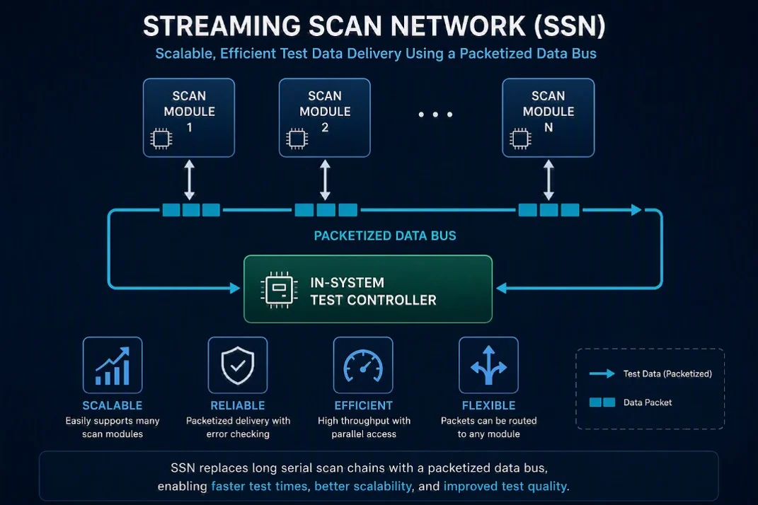
While AI could theoretically be used to optimize these traditional pin allocations, such an approach would only provide incremental improvements to a fundamentally limited system. The real breakthrough came from human engineering in the form of the Streaming Scan Network (SSN). Introduced as a packetized bus architecture for scan data delivery, SSN decoupled the core-level test requirements from the top-level IO.
By treating scan data as packets on a high-speed bus—much like data moving across a network—SSN allowed for unprecedented flexibility. This architecture enables software-based optimization of packets, allowing for changes in pattern sizes or combinations of cores to be tested in parallel without necessitating a physical redesign of the chip’s test infrastructure. This human-led innovation provided a much more powerful solution than simply applying AI to old methods, effectively setting a new "plan of record" for SoC scan data delivery across the industry.

The Chronology of Test Evolution and the Rise of Agentic AI
The timeline of DFT evolution reflects a steady progression from hardware-centric solutions to software-defined architectures, and finally, to AI-augmented workflows.
- The Traditional Era (Pre-2019): Focused on basic scan compression and boundary scan techniques. Test planning was manual and highly dependent on physical IO constraints.
- The SSN Revolution (2020–2022): The introduction of packetized data delivery changed the landscape, allowing for independent core testing and reduced routing congestion.
- The Operational Intelligence Shift (2023): The launch of In-System Test (IST) products allowed manufacturing-grade tests to be run in-situ, moving DFT beyond the factory floor and into the field.
- The Agentic AI Era (Late 2024 and Beyond): The upcoming integration of Agentic AI capabilities marks the next phase, where AI acts as a collaborative partner to the engineer, assisting in real-time planning, debugging, and optimization.
Agentic AI differs from standard automation in its ability to take initiative and perform multi-step reasoning. Later this year, Siemens EDA is set to provide these capabilities to assist engineers with the grueling task of Design Rule Checking (DRC) and violation resolution. When a DFT tool encounters a violation, the traditional process requires the engineer to manually investigate root causes, cross-reference documentation, and run iterative experiments to find a fix. An Agentic AI assistant accelerates this by identifying patterns in the violations, suggesting proven remediation strategies, and even pre-validating those fixes before presenting them to the human engineer for final approval.
Technical Deep Dive: AI as an Engineering Multiplier
The synergy between packetized data delivery (SSN) and AI provides capabilities that extend far beyond simple manufacturing tests. Because SSN is a flexible, software-defined infrastructure, it serves as the perfect playground for AI-driven optimization.
For instance, in a complex SoC with heterogeneous cores, the test data volume (TDV) required for each core varies significantly. AI algorithms can analyze the pattern requirements of each core in real-time to balance the load across the SSN bus. This ensures that no single core becomes a bottleneck, thereby minimizing the total time on the Automatic Test Equipment (ATE).
Furthermore, the "agentic" nature of new AI tools allows them to handle "debug" workflows that were previously considered too subjective for machines. In the event of a test failure on the production floor, an AI agent can correlate fail data with design schematics and layout information to pinpoint potential systematic defects. This capability is particularly vital as the industry moves toward advanced packaging nodes (such as 3D-IC and Chiplets), where the physical complexity of interconnects makes manual debugging nearly impossible.

From Manufacturing to Operational Intelligence: The Data Center Use Case
The implications of this technology are perhaps most visible in the context of "operational intelligence." A year ago, the industry saw the introduction of In-System Test (IST) technology, which allows the same test content used during manufacturing to be executed while the chip is in its final application.
Consider a modern hyperscale data center containing thousands of blade servers. In such an environment, hardware degradation is a constant threat. An agentic monitoring agent—integrated into the system’s firmware—can monitor various sensors, including bus functional monitors, temperature sensors, and voltage droop detectors. If a signal indicates a potential hardware anomaly, the AI agent can autonomously direct the system scheduler to run a specific group of tests via the IST hardware, often utilizing interfaces like PCIe.
This process allows for a proactive approach to hardware health:
- Identification: The AI detects a core that is underperforming or exhibiting timing errors.
- Verification: IST runs targeted diagnostics to confirm if the issue is a permanent hardware fault or a transient error.
- Mitigation: The system can decide to take a specific core out of service or flag the entire blade server for maintenance, avoiding costly Return Merchandise Authorizations (RMAs) and maintaining high availability for the data center’s clients.
Supporting Data and Industry Implications
The shift toward AI-enhanced DFT is supported by the staggering increase in chip complexity. According to industry reports, the number of transistors in high-end SoCs is doubling approximately every 24 months, while the number of test patterns required to ensure high quality is growing at an even faster rate. Without the efficiencies provided by SSN and AI, the "Cost of Test" could become a prohibitive percentage of the total product cost.
Analysis of current market trends suggests that companies adopting "Innovation-First" strategies see a significant reduction in Time-to-Market (TTM). By utilizing packetized delivery and AI-assisted debug, engineering teams have reported reductions in DFT implementation cycles by as much as 30% to 40%. This efficiency is a critical competitive advantage in sectors like mobile communications and consumer electronics, where product windows are extremely narrow.

Moreover, the integration of AI into the semiconductor lifecycle addresses the growing talent gap in the engineering sector. As veteran DFT engineers retire, the industry faces a shortage of experts capable of navigating the complexities of modern SoC design. Agentic AI serves as a "knowledge bridge," capturing best practices and institutional knowledge to empower less experienced engineers to perform at a higher level.
Official Perspectives and Future Outlook
Ron Press, Senior Director of Technology Enablement at Siemens EDA, emphasizes that the future of the industry is not about AI replacing human talent. "The future of DFT is not AI replacing engineers. Instead, it is AI amplifying engineering expertise," Press notes. This sentiment is echoed by Marc Hutner, Director of Product Management for Tessent Yield Learning, who highlights that the partnership between human innovation and AI extends across the entire semiconductor lifecycle—from initial design and validation to deployment and long-term field operation.
The consensus among these experts is that while AI can handle the "brute force" of optimization and data analysis, the "creative spark" required to invent entirely new architectures like SSN remains a uniquely human trait. The most impactful applications of this partnership have yet to be imagined, but the foundation is being laid today through the integration of packetized data networks and agentic intelligence.
In conclusion, the "Innovation First, AI Second" approach ensures that the semiconductor industry remains grounded in sound engineering principles while fully leveraging the transformative power of Artificial Intelligence. By focusing on architectural breakthroughs first, engineers create the robust infrastructures that AI needs to deliver on its promise of efficiency and reliability. As this synergy matures, it will continue to drive the next generation of semiconductor performance, ensuring that the chips powering our world are not only faster and more complex but also more reliable and easier to maintain throughout their entire operational life.
