
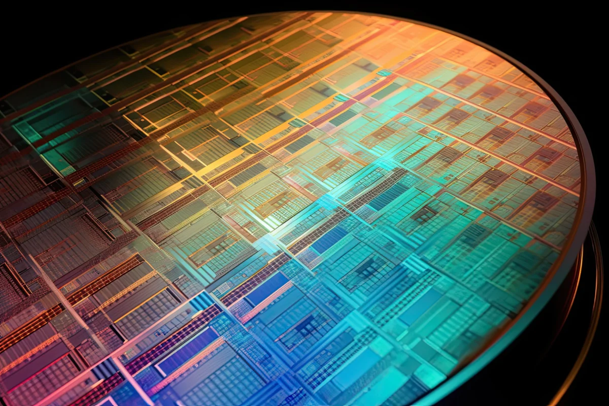

The rapid evolution of semiconductor manufacturing has reached a critical bottleneck: as transistors shrink toward the atomic scale, the physical limitations of conventional silicon-based architectures have become increasingly apparent. A collaborative research team comprising experts from the University of Illinois Urbana-Champaign, the National Energy Technology Laboratory, Argonne National Laboratory, and Monash University has unveiled a significant breakthrough in the integration of high-dielectric constant (high-κ) oxides onto two-dimensional (2D) semiconductor materials. Published in the October 2026 issue of Nature Communications, the study proposes a novel solution to the long-standing challenge of creating high-quality, uniform dielectric layers on materials that naturally lack dangling bonds, such as transition metal dichalcogenides (TMDs).
The Challenge of Surface Engineering in 2D Electronics
For decades, the semiconductor industry has relied on the native oxide of silicon (silicon dioxide) to serve as a high-quality gate dielectric. However, as the industry moves toward 2D semiconductors—materials just one or a few atoms thick—the interface between these materials and the necessary insulating oxide layers often suffers from defects. 2D semiconductors are chemically inert, meaning they lack the reactive sites required to bond with standard deposition precursors. Consequently, attempts to deposit high-κ oxides directly onto these surfaces often result in non-uniform growth, structural defects, and severe degradation of carrier mobility.
The researchers address this by introducing a carbon-dot monolayer assembly that acts as a van der Waals interfacial layer. By using these nanoscopic carbon structures, the team has successfully facilitated the growth of ultrathin, high-κ oxides that maintain their electrical integrity without damaging the underlying 2D semiconductor.
Chronology of the Breakthrough
The research project represents the culmination of several years of investigation into interfacial engineering. The timeline of this discovery follows a structured trajectory of material design, deposition optimization, and electronic validation:
- Early 2024: The collaborative team identified the "wetting" problem associated with atomic layer deposition (ALD) on 2D surfaces. Initial experiments focused on physical vapor deposition, which proved too damaging to the crystalline structure of the 2D sheets.
- Late 2024 – Mid 2025: Researchers pivoted toward self-assembled monolayers (SAMs). While effective in some scenarios, traditional SAMs struggled with thermal stability during high-temperature oxide deposition.
- Early 2026: The team successfully synthesized carbon-dot monolayers with high thermal stability and uniform density. This allowed for a seed layer that promotes uniform oxide nucleation.
- October 2026: The final validation of the integration process was published, demonstrating that the van der Waals interface allows for the deposition of high-κ oxides with minimal interface trap density, a critical metric for high-performance transistors.
Technical Mechanics: The Carbon-Dot Interface
The technical novelty of the study lies in the application of carbon-dot (CD) monolayers. Carbon dots are quasi-spherical nanoparticles, typically less than 10 nanometers in diameter. When organized into a monolayer on a semiconductor surface, they act as a "template" or "cradle" for the deposition of high-κ oxides, such as hafnium oxide (HfO₂).
Because the interaction between the carbon dots and the 2D semiconductor is governed by van der Waals forces—rather than covalent bonding—the electronic structure of the semiconductor remains undisturbed. This preserves the high carrier mobility inherent to 2D materials while providing the electrical insulation necessary for modern logic gates. Data from the study indicate that this assembly effectively suppresses tunneling currents, which are a primary source of power loss in miniaturized transistors.
Supporting Data and Performance Metrics
The experimental results presented in the paper highlight significant improvements in device performance compared to traditional deposition methods. The research team focused on two key metrics: interface trap density (Dit) and gate leakage current.

- Interface Trap Density: Devices fabricated with the carbon-dot interfacial layer exhibited a reduction in trap density by nearly an order of magnitude compared to direct-growth methods on untreated 2D surfaces. Lower trap densities are essential for reducing "noise" and improving the switching speed of transistors.
- Oxide Uniformity: Atomic Force Microscopy (AFM) analysis confirmed the formation of a continuous, pinhole-free oxide layer as thin as 2-3 nanometers. Achieving this level of uniformity at such extreme thinness is a major hurdle for scaling semiconductor manufacturing to the sub-2nm node.
- Carrier Mobility: Measurements indicated that the transistors retained over 90% of their intrinsic carrier mobility, confirming that the van der Waals interface does not introduce significant scattering centers that would otherwise degrade electronic transport.
Industry Implications and Future Outlook
The implications of this research extend across the semiconductor manufacturing value chain. As silicon approaches its physical limits, 2D materials are considered the most promising candidates for the next generation of electronic devices, particularly for high-frequency applications, flexible electronics, and ultra-low-power computing.
Industry analysts suggest that the ability to integrate high-κ dielectrics is the "missing link" for the commercialization of 2D transistors. If this process can be scaled to industrial wafer sizes, it would allow manufacturers to utilize existing Atomic Layer Deposition (ALD) infrastructure, significantly reducing the capital expenditure required to transition from silicon to 2D-based architectures.
"This approach demonstrates that interfacial engineering can be as important as the semiconductor material itself," noted one observer familiar with the study. "By using a van der Waals layer to bridge the gap between two disparate material systems, the researchers have opened a pathway for more complex, multilayered 2D electronic circuits."
Broader Impact on Semiconductor Scaling
The broader impact of this work relates to Moore’s Law and the continuous pursuit of smaller, faster, and more energy-efficient processors. Current high-performance computing (HPC) demands are putting unprecedented strain on thermal management and power density. By enabling thinner, more efficient gate stacks, the carbon-dot interface technology could contribute to a new generation of chips that operate at lower voltages while maintaining higher switching speeds.
Furthermore, the technique’s compatibility with low-temperature processes is particularly noteworthy. Many modern electronics, including those used in wearable technology and transparent displays, rely on flexible substrates that cannot withstand high-temperature processing. The researchers’ method, which is effective at lower thermal budgets, aligns well with the growing demand for flexible, high-performance electronics.
Conclusion and Scientific Consensus
The integration of carbon-dot monolayers as a van der Waals interfacial layer serves as a landmark development in the field of condensed matter physics and material science. By successfully navigating the trade-off between surface chemistry and electronic performance, the collaborative team has provided a scalable framework for future semiconductor innovation.
While the study is currently in the academic validation phase, its reliance on industry-standard deposition techniques suggests a high potential for technology transfer. Future work will likely focus on the long-term reliability and bias-temperature instability of these devices under sustained operation. As the global semiconductor industry looks toward the next decade of development, research into these atomic-scale interfaces will undoubtedly remain at the forefront of the technological roadmap, providing the necessary tools to sustain progress in an increasingly post-silicon era.
