
The semiconductor industry is currently navigating one of the most significant architectural transitions in its history as logic density pushes toward the 2-nanometer (nm) threshold and beyond. At these advanced nodes, the complexity of System-on-Chip (SoC) design has outpaced traditional verification methodologies, leading to a phenomenon known as the "DRC explosion." Design Rule Checking (DRC), once a straightforward validation step, has become a massive data management challenge. Early in the design cycle for 2nm chips, it is now common for initial DRC runs to generate hundreds of millions, and occasionally billions, of violations. This surge in data occurs precisely when design parameters are most fluid, with block interfaces, power grids, and routing constraints shifting through every iteration.
Managing these massive result sets is no longer a matter of simple manual review. In the traditional verification paradigm, engineering teams were forced to wait for a full DRC run to complete—often an overnight process—before they could begin analyzing the output. This serial "run-then-debug" cycle created significant bottlenecks, where a single catastrophic design error could hide thousands of smaller issues or render an entire day’s work obsolete. To maintain the aggressive time-to-market schedules required by the modern consumer electronics and high-performance computing (HPC) sectors, the industry is shifting toward real-time, AI-powered analysis platforms that integrate directly into the engineer’s active workflow.
The Technical Crisis of Sub-2nm Physical Verification
The transition to 3nm and 2nm nodes involves more than just shrinking dimensions; it introduces fundamentally new transistor architectures, such as Gate-All-Around (GAA) nanosheets, and increasingly complex multi-patterning and Extreme Ultraviolet (EUV) lithography requirements. Each of these technological leaps adds layers of new design rules. A decade ago, a process node might have had several hundred design rules; today, that number has climbed into the thousands, many of which are context-dependent and multi-layered.

As the number of rules grows, so does the volume of violations during the early stages of floorplanning and routing. In legacy DRC flows, verification tools often employed "error capping" to prevent system crashes or unmanageable file sizes. A tool might report only the first 1,000 instances of a specific violation. While this made the data sets smaller, it created a false sense of security. Engineers would fix the reported errors, only to find another 1,000 errors of the same type appearing in the next run. This "whack-a-mole" approach to debugging is increasingly unsustainable at the 2nm level, where the cost of a delayed tape-out can reach millions of dollars per day in lost opportunity and increased development overhead.
The Shift to Instance-Complete DRC Analysis
To address the limitations of sampled error reporting, the industry is moving toward "instance-complete" DRC analysis. This methodology ensures that every single violation is recorded and reported, regardless of how many times a specific block is instantiated or how deep it sits within the design hierarchy. By providing a comprehensive view of the error landscape from the first run, teams can identify systemic issues that affect the entire chip rather than addressing symptoms in isolation.
The shift to instance-complete reporting is made possible by modern data structures and file compression techniques. Traditional ASCII-based reporting formats, which were the industry standard for decades, are being replaced by binary and compressed formats capable of handling billions of data points without overwhelming the workstation’s memory. This allows for a "full-picture" diagnostic approach, where the design team can see the total scope of the challenge from day one of the integration phase.
Artificial Intelligence and the Compression of Debug Cycles
If an instance-complete run delivers one billion violations, the human element of the design team becomes the next bottleneck. No team of engineers can manually review a billion line items. This is where Artificial Intelligence (AI) and Machine Learning (ML) have become essential components of the Electronic Design Automation (EDA) toolkit.

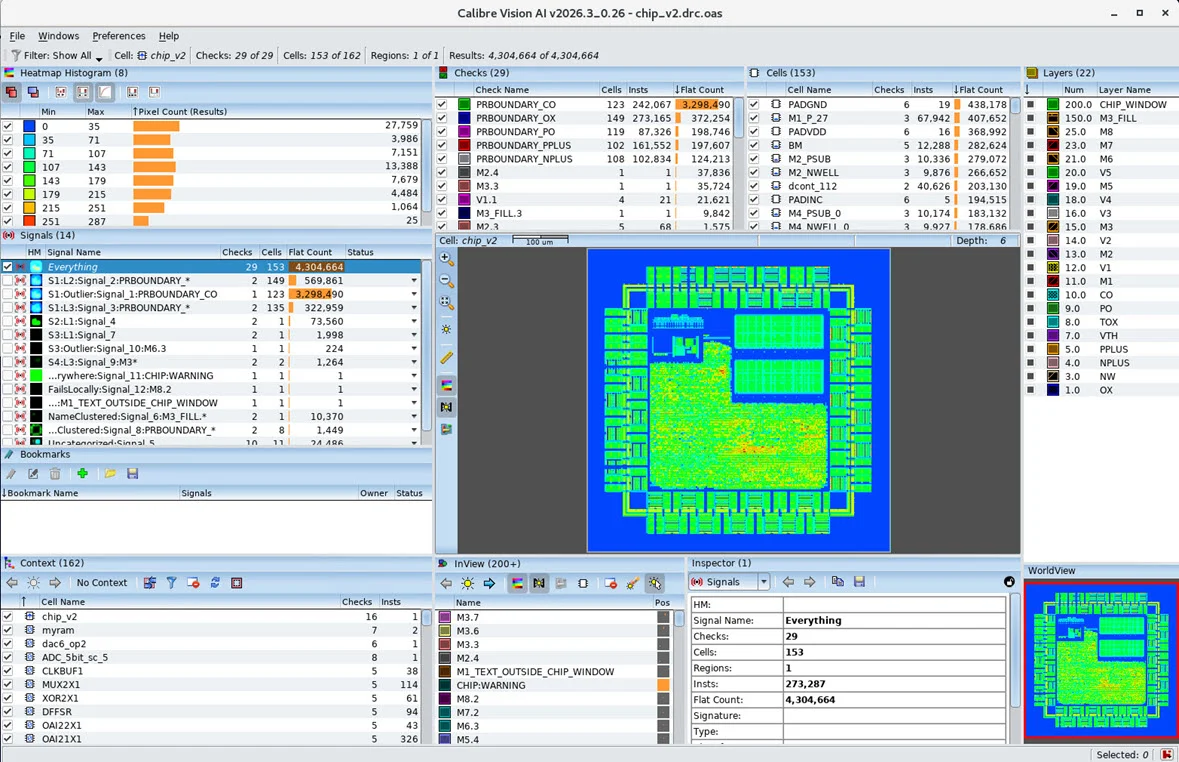
Modern platforms, such as Siemens’ Calibre Vision AI, utilize AI-driven grouping to transform raw data into actionable intelligence. These tools analyze the geometric patterns and spatial correlations of violations to cluster them into what are termed "Signals." A Signal represents a root cause—a specific design flaw or a misunderstood constraint—that may be responsible for millions of individual DRC markers.
Furthermore, AI algorithms can identify "Signatures," which are recurring patterns of violations across different areas of the SoC. If a specific library cell or a routing macro is causing errors in multiple blocks, the AI identifies the commonality. By fixing the signature at the source, the engineering team can eliminate vast swaths of violations simultaneously. This move from "point-fixing" to "root-cause resolution" is the primary driver of productivity gains in the 2nm era.
Parallelism and Incremental Workflows: A Chronological Shift
The chronology of the DRC process has historically been linear:
- Design Export (GDSII/OASIS)
- DRC Run (Hours/Days)
- Result Generation
- Manual Debug
- Iteration
The modern approach breaks this linearity through incremental results and parallel debugging. As the DRC engine processes the design, violations are streamed to an interactive dashboard in real-time. This allows engineers to begin addressing catastrophic errors—such as widespread power grid shorts or misaligned vias—within minutes of starting the run.

This parallel workflow is particularly vital for global design teams working across multiple time zones. With a centralized, real-time dashboard, a team in Asia can begin debugging the results of a run started by a team in North America, with the status of every violation tracked within the tool itself. This eliminates the need for fragmented communication methods like spreadsheets, email chains, or static slide decks, which often fail to keep pace with the speed of design changes.
Case Study: Impact on 3nm APU Development
The efficacy of these AI-driven methodologies was recently demonstrated in a real-world application by a leading semiconductor firm’s physical verification team. The team, which possesses over 20 years of experience across various process nodes, utilized Calibre Vision AI during the development of a custom 3nm Accelerated Processing Unit (APU).
Initially, the team faced a daunting verification environment: 3,400 different checks resulting in over 600 million violations. Using traditional methods, the team had to limit results per check just to keep the file sizes manageable, leading to the "surprise error" phenomenon where new violations would emerge only after previous ones were cleared. The visualization of these violations was slow, and identifying patterns in the massive ASCII database required labor-intensive manual effort.
Upon implementing an AI-guided DRC analysis platform, the team observed an immediate 40% to 50% reduction in their DRC iteration cycle time. This improvement was attributed to better file compression and the ability to visualize massive data sets quickly. However, as the team integrated advanced features—including incremental DRC output, hierarchical signature grouping, and global filtering—the performance gains increased to between 70% and 80%. This represented a 4x to 5x speedup over their previous established methods, allowing the team to achieve closure on a schedule that would have been impossible with legacy tools.

Broader Implications for the Semiconductor Industry
The move toward AI-integrated physical verification has broader implications for the semiconductor ecosystem. First, it lowers the barrier to entry for complex SoC design at advanced nodes. By automating the most tedious aspects of the debug process, smaller design teams can manage the complexity that was previously the sole domain of industry giants.
Second, it enhances the reliability of the final silicon. When engineers are not overwhelmed by "noise" in the DRC reports, they can focus their attention on critical "marginalities"—design features that technically pass the rules but are susceptible to yield loss during manufacturing. AI-powered filtering allows these subtle risks to be spotlighted, leading to higher initial yields and more robust chips.
Finally, this evolution represents a fundamental change in the role of the physical verification engineer. The focus is shifting from manual geometry correction to data science and systemic problem-solving. As nodes continue to shrink toward 14 Angstroms and beyond, the partnership between human intuition and AI-driven data processing will become the standard for all aspects of integrated circuit design.
Conclusion: The Path to 2nm Closure
The challenges of 2nm and sub-2nm design are formidable, but they are not insurmountable. The transition from a reactive, serial DRC process to a proactive, AI-driven, and instance-complete analysis framework is the key to maintaining the pace of innovation. By leveraging real-time results, persistent workflow tracking, and powerful global filters, design teams can transform the "DRC explosion" from a project-ending bottleneck into a manageable, organized process. As the industry moves forward, the ability to turn billions of violations into a handful of actionable insights will be the defining characteristic of successful SoC development.
