
The rapid evolution of artificial intelligence has fundamentally altered the architectural requirements of modern semiconductors, shifting the primary design constraint from transistor switching speeds to the stability of the on-die power delivery network. As AI workloads become increasingly "spiky," characterized by current demands that surge to hundreds of Amps within mere nanoseconds, the physical infrastructure responsible for delivering electricity to the silicon is reaching a breaking point. This phenomenon occurs precisely as advanced process nodes push operating voltages below 0.8V, leaving almost no margin for error. When the on-die power delivery network (PDN) fails to sustain the instantaneous current required by complex high-coincidence-matrix operations, the result is a functional bottleneck that effectively caps computational throughput and threatens system reliability.
The Physics of the AI Power Bottleneck
To understand the current crisis in chip design, one must look at the shifting landscape of power density. In traditional enterprise deployments, rack-level power density was typically measured in a few kilowatts. However, the surge in AI-optimized configurations has seen these requirements skyrocket toward and beyond 100kW per rack. This massive increase in power consumption is not a steady-state phenomenon but a highly dynamic one. GPU-based AI accelerators and specialized Tensor Processing Units (TPUs) cycle through distinct execution phases—prefill, decode, and idle—each with radically different power signatures.
The prefill phase, which involves loading and processing the initial input prompt, requires massive data movement and computational intensity. The decode phase, where each subsequent output token is generated, creates a different rhythm of power draws. These transitions produce load transients with low inertia, resulting in significant voltage surges and dips. Because these fluctuations occur at a high peak-to-idle ratio, conventional power delivery infrastructure, which was designed for more predictable and linear workloads, is increasingly inadequate. The result is a scenario where the hardware is physically capable of faster computation, but the electrical supply is too unstable to support it without risking logic errors.
The Limitations of Legacy Verification and Guard Banding
The primary challenge in addressing PDN instability lies in the transient and unpredictable nature of AI workloads. These events are both instructional and data-dependent, meaning they may only manifest as intermittent functional failures or subtle throughput degradations. Standard verification, characterization, and system-level testing methodologies often fail to catch these issues because they cannot easily replicate the exact sequence of instructions and data patterns that trigger a critical voltage droop.

Historically, chip designers have managed this uncertainty through "guard banding"—the practice of adding a voltage safety margin at the design stage to absorb worst-case transients. For example, if a chip is designed to operate at 0.75V but is known to experience 50mV droops, the designer might set the nominal operating voltage to 0.8V. While this ensures stability, it comes at a massive cost in power efficiency. Since power consumption in a CMOS circuit is proportional to the square of the voltage ($P propto V^2$), even a small increase in the guard band leads to significant heat generation and energy waste. In an era where multi-hundred-billion-dollar investments are flowing into AI-centric datacenters, these efficiency losses translate directly into millions of dollars in wasted operational expenditure and reduced hardware lifespan.
A New Paradigm: Correlating Physical and Functional Telemetry
To move beyond the limitations of guard banding, the industry is shifting toward a model of real-time observation and correlation. This requires a dual-layered approach: visibility into the logic-level behavior of the workload and high-resolution telemetry of the physical voltage at the transistor level. By aligning these two data streams, engineers can finally understand the causal relationship between specific software instructions and the resulting physical stress on the hardware.
The collaboration between Siemens EDA and Movellus represents a significant step forward in this domain. By integrating Siemens Tessent Embedded Analytics with Movellus Aeonic Insight, designers gain a holistic view of the chip’s health. The Siemens component provides functional monitors that observe on-chip behavior—such as transaction traffic across the interconnect—without interrupting normal operations. Meanwhile, the Movellus Aeonic Insight Droop Detector provides the physical layer of data, monitoring on-die voltage continuously and generating hardware triggers the moment a programmed threshold is crossed.
Chronology of the Integrated Monitoring Demo
To prove the efficacy of this correlated approach, Siemens and Movellus developed a demonstration system utilizing an AMD Zynq UltraScale+ FPGA platform. The chronology of the system’s operation illustrates how modern silicon can self-diagnose electrical stressors:
- Workload Initiation: Two RISC-V cores are tasked with running a target AI workload, simulating the high-intensity mathematical operations typical of neural network inference.
- Continuous Monitoring: The Siemens Tessent Bus Monitor tracks transaction traffic across the SoC interconnect, while the Status Monitor keeps tabs on the overall system health. Simultaneously, the Movellus Droop Detector monitors the on-die voltage at the transistor level.
- Threshold Violation: As the RISC-V cores hit a peak execution cycle, a sudden surge in current causes a localized voltage droop. The Droop Detector identifies that the voltage has crossed a pre-defined safety threshold.
- Hardware Triggering: Within nanoseconds, the Droop Detector fires a hardware trigger directly to the Tessent Embedded Analytics infrastructure.
- Data Capture: The system captures a "snapshot" of both the core execution state and the interconnect activity at the exact moment the voltage event occurred.
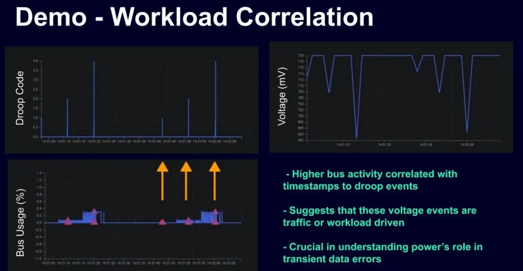
- Analysis and Alignment: The resulting data provides a time-aligned trace where peaks in workload intensity are perfectly mapped to voltage fluctuations.
This demonstration proves that voltage stress is no longer a "black box" event. Engineers can see precisely which workload conditions drove the stress, where on the die it occurred, and the exact severity of the dip.

Supporting Data: The Impact of Precise Calibration
The implications of this data-driven approach are quantifiable. In high-performance computing environments, reducing the voltage guard band by as little as 5% can result in a 10% reduction in total power consumption. For a large-scale datacenter operating at 50 megawatts, this represents a 5-megawatt saving—enough to power thousands of homes or, more importantly, to provide additional thermal headroom for increased computational density.
Furthermore, the ability to detect "near-miss" events—where a voltage droop almost reaches a failure threshold—allows fleet operators to implement predictive maintenance. Rather than waiting for a GPU to crash or produce "silent data corruption" (SDC), operators can adjust workload distribution or throttle specific cores based on real-time PDN health data. This granular telemetry is essential for maintaining the "five nines" (99.999%) of reliability expected in enterprise-grade AI infrastructure.
Industry Reactions and Strategic Implications
Market analysts suggest that the shift toward integrated physical and functional monitoring is a mandatory evolution for the sub-5nm era. As the industry moves toward 3nm and 2nm nodes, the "noise" in the power delivery network becomes indistinguishable from the signal, making traditional external voltage sensing nearly useless.
Major hyperscalers and chip designers are reportedly looking at these embedded analytics as a way to "bin" chips more effectively. By testing how individual pieces of silicon respond to specific AI instruction sequences, manufacturers can categorize chips not just by their clock speed, but by their electrical resilience. This allows for more aggressive performance tuning in high-quality silicon while maintaining safety in average units.
Broader Impact and Future Outlook
The convergence of physical and functional observability marks the end of the "set it and forget it" era of chip design. In the future, AI chips will likely feature closed-loop systems where the PDN monitors and the functional monitors work together to dynamically adjust clock speeds and voltages in real-time, responding to the specific needs of the software being executed.

For the broader AI industry, this technology addresses one of the most significant barriers to scaling: the power wall. By allowing infrastructure to run closer to its physical limits without crossing into instability, companies can maximize their return on investment in silicon. The partnership between Siemens and Movellus highlights a growing trend where EDA (Electronic Design Automation) tools are no longer just used for the design phase but are becoming permanent, "on-chip" residents that safeguard the device throughout its entire lifecycle.
As AI workloads continue to grow in complexity and intensity, the ability to correlate what a chip is doing with how it is feeling—electrically speaking—will be the difference between a high-performing fleet and a costly, unstable investment. The transition from inferred stress to traceable telemetry is not just a technical upgrade; it is a fundamental requirement for the next generation of global computing infrastructure.