
The global semiconductor industry is currently navigating one of the most significant architectural shifts in its history as it moves beyond the 3nm node toward sub-2nm regimes. Central to this evolution is the transition from conventional Gate-All-Around (GAA) nanosheets to complementary field-effect transistors (CFETs) and the integration of Backside Power Delivery Networks (BSPDN) utilizing buried power rails (BPRs). While these innovations promise to maintain the trajectory of Moore’s Law by providing unprecedented device density and improved power-performance-area (PPA) metrics, they introduce a paradigm shift in electronic design automation (EDA). Specifically, the task of parasitic extraction—modeling the unintended resistance, capacitance, and inductance within a circuit—has become exponentially more complex. Siemens Calibre xACT has emerged as a critical solution in this landscape, offering unified extraction tools designed to handle the intricate geometries of vertical transistor stacking and backside metal stacks.
The Architecture of Tomorrow: CFET and Buried Power Rails
To understand the extraction challenges, one must first grasp the physical transformation of the transistor. For decades, semiconductor scaling relied on lateral shrinking. When planar transistors hit a wall, the industry moved to FinFETs, and more recently, to GAA nanosheets. However, even nanosheets face "area scaling" limits because the n-type and p-type transistors are still placed side-by-side on the silicon wafer.
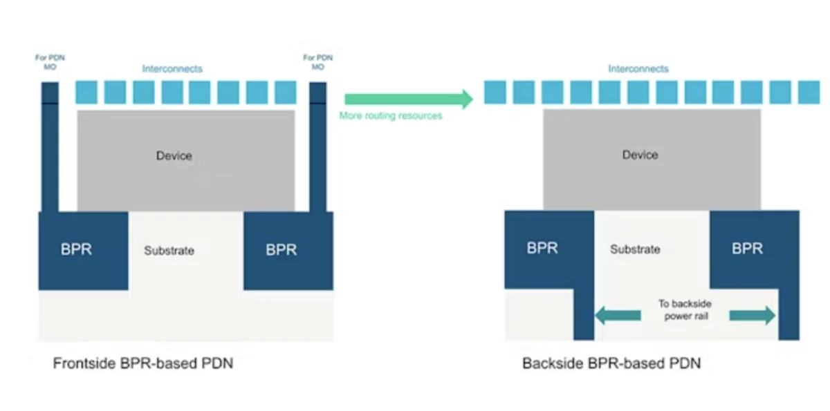
The CFET architecture breaks this horizontal constraint by vertically stacking the n-FET and p-FET on top of each other. This vertical integration theoretically allows for a 50% reduction in the standard cell area, effectively doubling the logic density without requiring a proportional shrink in lithographic features. Complementing this is the Buried Power Rail (BPR) and Backside Power Delivery. In traditional designs, both signals and power are routed through the front-side metal layers (M0, M1, etc.). This creates immense congestion and "IR drop" (voltage drop) as power must compete for space with high-speed signal lines. BPR moves the heavy power distribution lines beneath the transistors, into the silicon substrate, and connects them to the back of the wafer. This separation of power and signal delivery is essential for the high-current demands of modern AI accelerators and high-performance computing (HPC) chips.
A Chronology of Transistor Evolution and the Road to 3nm
The path to CFET and BSPD has been marked by several distinct eras of semiconductor engineering. Understanding this timeline is vital for contextualizing why current extraction methods must evolve.
- The Planar Era (Pre-2011): Transistors were two-dimensional. Extraction was relatively straightforward, focusing on lateral capacitance and simple wire resistance.
- The FinFET Revolution (2011–2022): Led by Intel’s 22nm node, the industry moved to 3D "fins." This introduced the need to model 3D parasitic capacitance between fins, but the n-type and p-type devices remained side-by-side.
- The GAA/Nanosheet Transition (2022–Present): Introduced at the 3nm node by Samsung and adopted for 2nm by TSMC and Intel, GAA nanosheets provide better electrostatic control. Extraction tools had to begin accounting for complex "inner spacer" capacitance.
- The CFET and Backside Era (Expected 2025–2030): This represents the current frontier. The integration of CFET and BPR requires tools that can simultaneously model the front-side signal stack and the back-side power stack, connected through Through-Silicon Vias (TSVs) or "PowerVias."
Technical Challenges in Parasitic Extraction
Parasitic extraction is the process of calculating the electrical "noise" and resistance inherent in the physical materials of a chip. At 3nm and below, these parasitics are no longer negligible; they can account for more than 50% of the total delay in a high-performance circuit.
Interface Resistance and Vertical Stacking
In a CFET structure, the vertical stacking of transistors creates new interfaces. The contact resistance between the source/drain regions and the vertical interconnects is highly sensitive to process variations. Traditional extraction tools often treat these as simplified 2D structures, but CFETs require a full 3D volumetric analysis. Modeling the interface resistance accurately is paramount because even a few ohms of unexpected resistance can lead to timing violations in a 2GHz+ processor.
Non-Manhattan Routing and Complex Geometries
Modern routing is no longer strictly "Manhattan" (rectilinear). To optimize space around BPRs and TSVs, designers are increasingly using diagonal or curved routing. Furthermore, the presence of TSVs—which penetrate the substrate to connect the backside power network to the front-side devices—introduces massive parasitic elements that were previously only seen in advanced packaging. Calibre xACT is designed to handle these non-standard geometries by using advanced field solvers that can calculate electromagnetic properties for any arbitrary shape.
RLCK Extraction: The Inductance Factor
At high frequencies, simple Resistance (R) and Capacitance (C) modeling is insufficient. Engineers must now account for Inductance (L) and Mutual Inductance (K). This is known as RLCK extraction. As AI chips push clock speeds higher, the magnetic coupling between dense signal lines and the new backside power rails can cause signal integrity issues. The BPR, being a large metal structure close to the device, acts as a significant inductor that can influence nearby logic gates.
Supporting Data: The Impact of Backside Power
Industry research from leading foundries and EDA providers like Siemens suggests that the move to Backside Power Delivery is not merely an option but a necessity. Data indicates that:

- IR Drop Reduction: BSPD can reduce the voltage drop (IR drop) by as much as 30% compared to traditional front-side delivery. This allows chips to run at lower voltages, saving power, or higher frequencies at the same power envelope.
- Area Efficiency: The combination of CFET and BPR can provide a logic density boost of 1.5x to 2.0x over standard GAA nanosheet designs at the same lithographic node.
- Routing Congestion: By moving power to the back, the number of available routing tracks on the front side increases by approximately 20% to 30%, simplifying the physical design of complex SoCs (Systems on Chip).
Industry Response and Official Perspectives
The semiconductor ecosystem—comprising foundries like TSMC, Intel, and Samsung, alongside EDA giants like Siemens—has reached a consensus that a "unified" extraction flow is the only path forward.
Siemens Digital Industries Software has positioned Calibre xACT as a bridge between the front-end-of-line (FEOL) and back-end-of-line (BEOL). By providing a single platform that handles both the device-level parasitics of the CFET and the macro-level parasitics of the backside power network, Siemens aims to reduce the "margin of error" that typically forces designers to over-engineer their chips, which wastes area and power.
Inferred industry sentiment suggests that design teams are particularly concerned about "sign-off" reliability. In the past, front-end and back-end teams often worked in silos. However, with CFETs, the device and the power network are physically and electrically intertwined. "The era of separating the transistor from the wire is over," is a common refrain among senior integration engineers. The requirement for RLCK extraction that covers the entire 3D stack is now a mandatory checkmark for any 2nm design start.
Workflow Setup and Reliability Modeling
Implementing a successful CFET/BPR design requires a rigorous workflow setup. According to technical documentation regarding Calibre xACT, the process begins with precise interface resistance modeling. This involves:
- Defining the Stack: Engineers must define the exact materials and dimensions of the CFET stack, including the BPR and the backside metal layers.
- Field Solver Integration: Using a field solver to create a "golden" reference for the most sensitive parts of the circuit, such as the clock tree and the power grid.
- Unified Extraction: Running the extraction tool to generate a comprehensive netlist that includes all R, L, C, and K components.
- Reliability Analysis: Assessing Electromigration (EM) and Voltage Drop (IR) using the extracted parasitics to ensure the chip will not degrade over its expected 5-to-10-year lifespan.
This workflow is particularly vital for AI accelerators used in data centers. These chips operate at high temperatures and high current densities. If the extraction tool underestimates the resistance of a buried power rail, the resulting heat could lead to premature chip failure.
Broader Impact and Implications for the Global Economy
The successful deployment of CFET and BSPD technology has implications far beyond the engineering lab. As the backbone of the digital economy, semiconductor performance dictates the ceiling for AI development, autonomous driving, and telecommunications.
For the AI sector, the efficiency gains from CFETs mean that the next generation of Large Language Models (LLMs) could be trained on hardware that consumes significantly less power per TFLOP (teraflop). In the mobile space, these technologies could lead to smartphones with multiday battery life despite having more powerful processors.
However, the complexity of these designs also raises the barrier to entry. Only companies with access to advanced EDA tools like Siemens Calibre xACT and the financial capital to tape out 2nm/3nm designs will be able to compete at the leading edge. This could lead to further consolidation in the chip design industry, where "mega-firms" dominate the high-performance market while smaller players focus on legacy nodes.
Conclusion
The integration of CFETs and Buried Power Rails represents a turning point in semiconductor history, marking the transition from 2D scaling to true 3D integration. While the physical benefits of this shift are clear—higher density, better power efficiency, and improved performance—the engineering hurdles are substantial. Parasitic extraction, once a secondary concern, has moved to the forefront of the design cycle.
Tools like Siemens Calibre xACT are no longer just "calculators" for resistance and capacitance; they are essential navigation systems for engineers venturing into the sub-3nm landscape. By providing unified modeling for front and back metal stacks, addressing the nuances of interface resistance, and enabling high-fidelity RLCK extraction, these tools ensure that the next generation of devices is not only possible but reliable and efficient. As the industry looks toward 2025 and beyond, the ability to accurately model the invisible parasitics of the 3D transistor will be the deciding factor in the success of the world’s most advanced electronic systems.