
The semiconductor industry has reached a critical inflection point where the limitations of physics are dictating the future of architectural design. As High-Performance Computing (HPC) and Artificial Intelligence (AI) accelerators push power densities toward 1kW and beyond, the heat generated by billions of rapidly switching transistors has become the primary bottleneck for performance scaling. The traditional methods of heat dissipation, once considered a secondary concern handled late in the design cycle, have proven inadequate for the era of multi-die packages and 3D integrated circuits (3D-ICs). To address these challenges, engineers are adopting a multidisciplinary approach that combines advanced finite element modeling, artificial intelligence, and real-world experimental validation to ensure the reliability and efficiency of the world’s most powerful chips.
The Paradigm Shift: From Monolithic to Multi-Die Thermal Management
For decades, thermal management was a relatively straightforward exercise. During the era of monolithic chip packaging, where a single silicon die was housed within a single integrated circuit (IC) package, engineers relied on shorthand equations and thermal resistance values to approximate junction temperatures ($T_j$). By calculating the resistance of the substrate, lid, and underfill, designers could ensure that the maximum temperature did not exceed the industry-standard limits—typically 105°C for CMOS or 85°C for DRAM.
However, the transition to multi-die packaging, driven by the need for greater density and the "chiplet" revolution, has rendered these shorthand methods obsolete. In modern high-end GPUs and microprocessors, thermal modeling has moved from the final stages of design to the very beginning of the prototyping phase. This shift is part of a broader industry trend known as System-level Technology Co-optimization (STCO).
According to industry leaders at Amkor Technology and Synopsys, thermal considerations now dictate the physical placement of chiplets. Designers must account for thermal coupling—the phenomenon where heat from one chiplet migrates to its neighbor—and prevent thermal runaway, a destructive cycle where rising heat increases power leakage, which in turn generates more heat. Failure to address these issues early in the design cycle often results in catastrophic strategic errors, requiring expensive design restarts or the implementation of prohibitively costly cooling solutions.

The Role of AI and Adaptive Meshing in Simulation
To visualize the complex thermal conduction profiles within a 3D-IC, engineers employ Finite Element Method (FEM) simulations. This process involves "meshing," where the chip and its package are segmented into thousands or millions of small polygons to solve heat flow equations. The challenge lies in balancing computational speed with analytical accuracy.
A fine mesh provides high resolution and captures localized hotspots, but it requires immense computational resources. Data from AMD indicates that a 200µm mesh size can increase solver time by approximately 1,200% compared to a 1,000µm mesh. Conversely, a coarse mesh is fast but risks missing "peak temperatures" that could lead to local failures, such as the melting of solder bumps or the degradation of interconnects.
To solve this dilemma, the industry is increasingly turning to AI-driven adaptive meshing. AI algorithms are used to predict where hotspots are likely to occur based on intended workloads. The simulation software then applies a finer mesh to those specific "hot zones" while maintaining a coarser mesh in cooler regions. This targeted approach allows engineers to achieve the precision of a 20µm or 100µm mesh at critical junctions without the prohibitive time penalty of a uniform high-resolution mesh.
Bridging the Gap Between Simulation and Reality
While simulation technology has advanced rapidly, the industry maintains a healthy skepticism of models that lack empirical validation. Discrepancies between a virtual model and a physical prototype can arise from unforeseen material behaviors or the fast time constants governing electrical switching. For example, a 1GHz microprocessor generates a billion activity vectors every second, creating a dynamic thermal environment that is difficult to replicate in a static simulation.
To bridge this gap, organizations like Fraunhofer IIS’s Engineering of Adaptive Systems Division have developed active thermal test platforms. Unlike the passive test structures of the past, these new platforms use wafers equipped with programmable digital heating blocks and high-resolution sensors. These "heater dies" allow researchers to emulate realistic, shifting AI workloads in a laboratory setting.

By selecting the size and arrangement of these blocks, engineers can recreate the specific power densities of a next-generation GPU. This real-world testing provides vital data on how heat propagates through new materials, such as those used in hybrid bonding or backside power delivery networks (PDN). These experimental "thermal vehicles" are now used throughout the product lifecycle, from initial floorplanning to post-deployment monitoring on customer boards.
Mechanical Implications: Stress, Warpage, and CTE Mismatch
Thermal management is not merely a matter of keeping temperatures low; it is also about managing the physical integrity of the package. Different materials within a chip—silicon, copper, dielectrics, and organic substrates—expand and contract at different rates when heated. This Coefficient of Thermal Expansion (CTE) mismatch creates significant mechanical stress.
In 3D-IC stacking, where multiple layers of silicon are bonded together, this stress can lead to "warpage"—the physical bending of the interposer or the die. Engineers must now model Von Mises forces, which represent the internal stresses at every point in the assembly. Stiffer materials might resist warpage but suffer from higher internal stresses that can cause cracking, while more flexible materials might warp to the point of breaking electrical connections. Modern EDA (Electronic Design Automation) tools are now integrating mechanical and thermal analysis into a single workflow, recognizing that the two are inextricably linked.
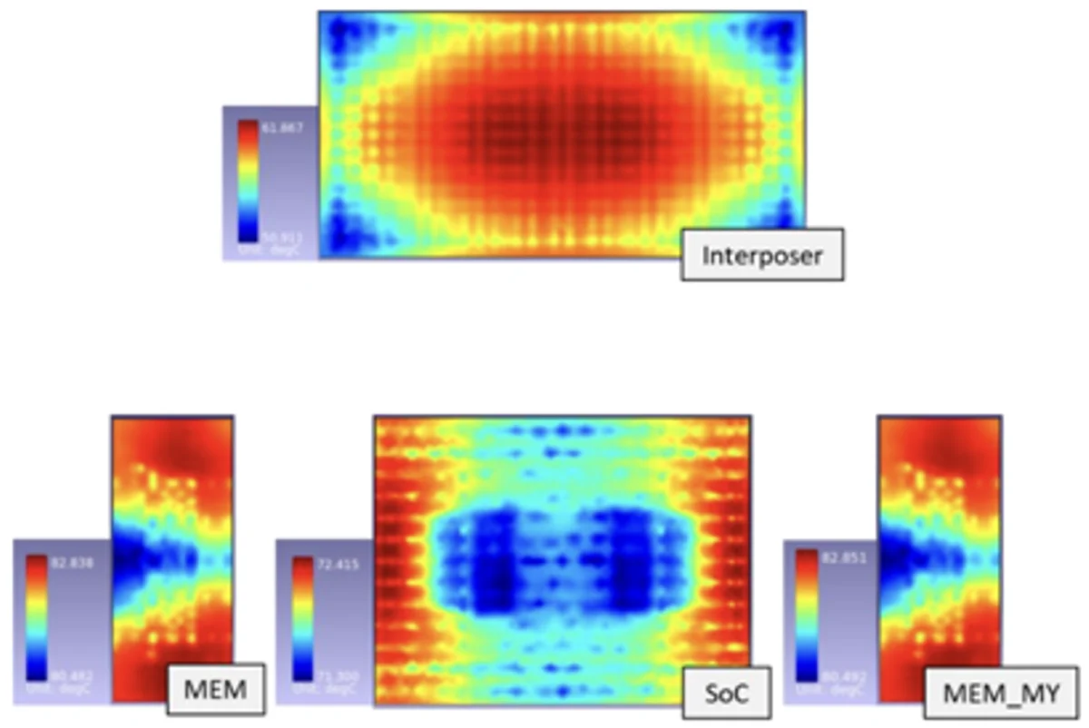
Case Study: Solving the 3D GPU-HBM Thermal Crisis
A recent research initiative led by imec provides a concrete example of how STCO can overcome extreme thermal barriers. The study examined a 3D configuration involving four 12-high High Bandwidth Memory (HBM) stacks placed directly atop a GPU. In its initial state, the GPU dissipated 414 watts and the HBMs 40 watts each, leading to a junction temperature exceeding 140°C—well beyond the point of failure.
To mitigate this, the imec team implemented a series of technology-level changes:

- Redundancy Removal: The base logic dies of the HBM stacks were removed to improve thermal coupling.
- Thermal Silicon Integration: Molding compounds were replaced with "thermal silicon" to enhance vertical and lateral heat spreading.
- Advanced Cooling: The team utilized microchannel or jet impingement cooling on the lid side, capable of removing 30kW/m²K.
- Frequency Scaling: By reducing the GPU’s core frequency and optimizing the floorplan, the peak temperature was eventually brought down to 70.8°C.
This result is significant because it brings the thermal profile of a 3D architecture in line with that of a 2.5D implementation, proving that 3D stacking is thermally viable for AI workloads if managed through rigorous co-design.
The Impact of Backside Power and Hybrid Bonding
As the industry moves toward sub-2nm nodes, new manufacturing processes like backside power distribution networks (PDN) and hybrid bonding are becoming standard. Backside PDN involves moving the power delivery lines to the rear of the wafer to reduce congestion and resistive losses. While this solves many interconnect problems, it removes a traditional path for heat dissipation, effectively "trapping" heat within the silicon layers.
Similarly, hybrid bonding—which uses direct copper-to-copper connections between stacked dies instead of traditional bumps—increases the density of heat-generating interconnects. Engineers are responding by developing "power-aware" floorplanning, where the placement of functional blocks is optimized not just for signal speed, but for the efficient routing of heat toward the cooling interface.
Conclusion and Future Outlook
The "thermal wall" is perhaps the greatest challenge facing the continued advancement of Moore’s Law in the AI era. As power densities exceed the 1kW threshold, the industry is moving away from reactive cooling and toward proactive, simulation-heavy design. The integration of AI into thermal modeling, the use of programmable thermal test vehicles, and the adoption of STCO principles are no longer optional; they are requirements for survival in the high-performance silicon market.
Looking forward, the industry is exploring even more radical solutions, including immersive liquid cooling and the integration of microfluidic channels directly into the silicon substrate. While these technologies remain in the developmental phase, the foundation being laid today through advanced modeling and experimental validation will determine the reliability and performance of the computing infrastructure that powers the next decade of AI innovation. The goal is no longer just to "beat the heat," but to master it as a fundamental variable in the architecture of the future.