
The global semiconductor industry is currently navigating a transition from the nanometer scale toward the "Angstrom Era," a shift that necessitates radical innovations in material science, metrology, and packaging. As traditional silicon-based manufacturing approaches the physical limits of Moore’s Law, researchers are increasingly looking toward two-dimensional (2D) materials, artificial intelligence, and novel chemical bonding techniques to overcome the bottlenecks of plasma etching, atomic-level defect identification, and environmental durability. Three recent breakthroughs—a 2D hard mask material from Penn State, an AI-driven defect classification model from MIT, and an extreme-environment photonic packaging method from NIST—represent a tripartite leap forward in the reliability and precision of next-generation microelectronics.
The Evolution of Lithography: 2D Chromium Oxychloride as a Hard Mask
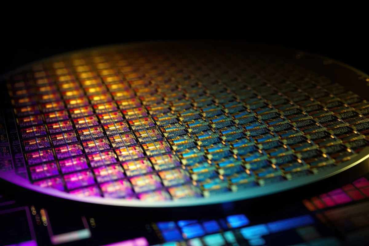
As integrated circuits (ICs) become more densely packed, the aspect ratio of the features etched into silicon wafers becomes a critical engineering challenge. Traditional hard masks, typically made of silicon dioxide or metallic films, must be thick enough to withstand the corrosive environment of plasma etching. However, as features shrink, thick masks become unstable, leading to pattern collapse or geometric distortions. Researchers from Pennsylvania State University and the University of Chemistry and Technology Prague have identified chromium oxychloride (CrOCl), a 2D layered material, as a potential solution to this structural bottleneck.
The Mechanism of Plasma Resistance
The efficacy of CrOCl lies in its unique "lasagna-like" atomic structure. Unlike bulk materials that erode uniformly under ion bombardment, CrOCl reacts with plasma to form a chemically inert passivation layer on its surface. Ziheng Chen, a doctoral candidate at Penn State, notes that this layer shields the underlying material from further reaction, allowing a significantly thinner layer of CrOCl to serve as an effective barrier compared to conventional materials.
In experimental trials, the research team demonstrated that 2D CrOCl can be patterned independently and subsequently transferred onto a variety of substrates, including glass and flexible plastics. This transferability is vital for the development of flexible electronics and wearable technology, where high-temperature deposition of traditional masks would destroy the underlying substrate.
Self-Smoothing and Vertical Precision
One of the most significant findings in the study of CrOCl is its behavior under repeated plasma exposure. In traditional etching, ion bombardment often increases surface roughness, which leads to "micro-masking"—a phenomenon where small particles or rough patches shield parts of the wafer, resulting in uneven, jagged features. CrOCl, conversely, exhibits a self-smoothing property.
According to Pranavram Venkatram, another lead researcher on the project, the plasma bombardment effectively "peels away" the rougher, disorganized regions of the CrOCl, revealing a pristine, atomically smooth surface beneath. This smoothness prevents the redeposition of etching byproducts, enabling the creation of sharper, more vertical structures. Such precision is essential for high-aspect-ratio features required in 3D NAND flash memory and advanced logic gates.
AI and Neutron Scattering: A New Paradigm in Defect Metrology
While material innovations like CrOCl improve the "how" of manufacturing, breakthroughs in artificial intelligence are revolutionizing the "what" of quality control. In the semiconductor world, defects are both a tool and a hindrance. Controlled defects, known as dopants, give semiconductors their electrical properties, but unintended point defects can ruin a chip’s performance. Identifying these defects at the atomic scale has historically required invasive or destructive techniques.
The Foundational Model for Materials
A collaborative effort between MIT and Oak Ridge National Laboratory (ORNL) has resulted in the development of an AI foundational model capable of identifying and quantifying defects using non-invasive neutron-scattering data. This model was trained on a massive dataset encompassing 2,000 different semiconductor materials and covers 56 elements from the periodic table.
The model utilizes a multihead attention mechanism, the same architecture that powers large language models like ChatGPT. Instead of processing text, however, this model processes vibrational spectra. By comparing the data from a material under test against a baseline of defect-free structures, the AI can simultaneously detect up to six different types of point defects, identifying both the specific dopants used and their exact concentrations.
Beyond the Human Eye
The complexity of neutron-scattering data often renders it indecipherable to human analysts. Mingda Li, associate professor at MIT, emphasized that while defect signals may look identical to the human eye, the pattern recognition capabilities of the AI can discern the "ground truth" within the noise. This capability is particularly important as the industry moves toward "defect engineering," where the precise placement of atoms is used to tune the properties of materials for quantum computing and high-power electronics.
While neutron scattering provides high-fidelity data, the researchers acknowledge that the specialized facilities required for such measurements (like the Spallation Neutron Source at ORNL) are not practical for high-volume manufacturing lines. Consequently, the team is currently adapting the model to work with Raman spectroscopy, a common, light-based technique already used in many semiconductor fabrication facilities.
Hardening Photonics: NIST’s Hydroxide Catalysis Bonding
As data demands increase, the industry is shifting from traditional electronic interconnects to silicon photonics, which use light (photons) instead of electricity (electrons) to transmit information. However, photonic chips have traditionally been "fragile," particularly at the interface where the optical fiber meets the chip. Standard adhesives, such as epoxies, are susceptible to thermal expansion, outgassing in vacuums, and degradation under radiation.
Molecular Fusion via HCB
Researchers at the National Institute of Standards and Technology (NIST) have developed a packaging process that replaces organic glues with an inorganic chemical bond. The technique, known as hydroxide catalysis bonding (HCB), involves applying a small amount of sodium hydroxide solution to the surfaces of the optical fiber and the photonic chip. This triggers a chemical reaction that fuses the two surfaces at the molecular level, creating a glass-like bond.
This bond is fundamentally different from traditional adhesives because it becomes an integral part of the material structure. NIST physicist Nikolai Klimov stated that the resulting bond is as resilient as the optical fiber itself. This allows photonic integrated circuits (PICs) to operate in environments that were previously inaccessible, such as the cryogenic temperatures required for quantum sensors, the high-radiation environments of nuclear reactors, and the extreme thermal cycles of deep space.
Scaling for Industrial Production
The primary hurdle for HCB is currently the time required for the bond to fully cure, which can take several days. For the technique to be viable for large-scale industrial manufacturing, this window must be compressed. The NIST team is currently investigating methods to accelerate the chemical reaction without compromising the integrity of the bond. If successful, this could lead to a new class of "ruggedized" photonic chips capable of supporting high-speed communication in the most hostile environments on and off Earth.
Chronology of Development and Future Milestones
The timeline for these technologies suggests a phased integration into the semiconductor ecosystem over the next five to ten years.
- Phase I (2024–2026): Discovery and Laboratory Validation. The initial papers published in Nature Materials, Matter, and Photonics Research establish the physical and chemical viability of CrOCl masks, AI defect modeling, and HCB packaging.
- Phase II (2027–2029): Scaling and Adaptation. This period will focus on growing CrOCl uniformly across 300mm wafers, a necessary step for industrial adoption. Simultaneously, the MIT AI model will be transitioned to Raman spectroscopy platforms for in-line fab use.
- Phase III (2030 and beyond): Industrial Deployment. Ruggedized photonic chips using HCB are expected to debut in satellite constellations and next-generation nuclear monitoring systems, while CrOCl masks may become standard in the production of sub-2nm logic nodes.
Broader Impact and Industrial Implications
The convergence of these three technologies addresses the three pillars of modern semiconductor manufacturing: precision, intelligence, and durability.
The use of 2D materials like CrOCl represents a shift away from "bulk" chemistry toward "surface" chemistry. By using materials that are only a few atoms thick, manufacturers can maintain the fidelity of complex patterns at scales where traditional materials fail. This will be a cornerstone of the transition to Angstrom-scale devices.
The MIT/ORNL AI model represents the maturation of "Industry 4.0" in the semiconductor space. By providing a non-destructive way to verify atomic structures, companies can reduce waste and accelerate the development of new materials. The ability to quantify defects with such precision will be particularly transformative for the wide-bandgap semiconductors (like silicon carbide and gallium nitride) used in electric vehicles and renewable energy grids.
Finally, the NIST packaging breakthrough ensures that the high-performance chips of the future are not limited to climate-controlled data centers. By hardening photonics for extreme environments, NIST is enabling a new era of "edge computing" in space and heavy industry, where data must be processed locally under intense physical stress.
In conclusion, these advancements signify a move toward a more resilient and precise semiconductor infrastructure. While challenges remain in scaling these laboratory successes to global high-volume manufacturing, the foundational science provides a clear roadmap for the next decade of microelectronic evolution. The synergy between 2D materials, AI-driven metrology, and molecular-level packaging will likely define the high-performance computing landscape of the 2030s.