
The escalating complexity of modern system-on-chip (SoC) designs has pushed traditional verification methodologies to their breaking point, with verification activities now consuming up to 70% of the total effort in a semiconductor project. According to the latest Cadence SoC Verification report, this lopsided allocation of resources underscores a fundamental crisis in hardware development: while design tools have evolved to handle billions of transistors, the processes used to ensure those transistors function correctly have struggled to keep pace. The industry is currently witnessing a paradigm shift as Artificial Intelligence (AI) and Large Language Models (LLMs) are integrated into the Electronic Design Automation (EDA) stack, enabling a "shift left" strategy that empowers designers to take on verification tasks earlier in the lifecycle, fundamentally altering the economics of chip manufacturing.
The Verification Bottleneck and the Cost of Late-Stage Discovery
In the traditional "waterfall" model of semiconductor development, a distinct wall often exists between design engineers and Design Verification (DV) engineers. Designers focus on the Register Transfer Level (RTL) code to implement functionality, while DV teams build complex environments to stress-test that code. This separation creates a significant bottleneck during the debugging and coverage closure phases. When a bug is discovered late in the cycle—often during subsystem or full-chip integration—the cost of remediation is exponential.
Data from the Wilson Research Group indicates that only about one-quarter of integrated circuit (IC) projects achieve first-pass silicon success. The primary cause of these failures is functional logic errors. The iterative loop of "design-test-fail-debug-rewrite" is the most time-consuming aspect of the project. Every time a designer has to wait for a DV report, and every time a DV engineer has to wait for an RTL fix, the project’s time-to-market (TTM) slips. In an industry where being first to a new process node (such as 3nm or 2nm) can determine market leadership, these delays are increasingly unacceptable.
A Chronology of Verification Evolution
To understand the impact of AI, it is necessary to view the historical progression of verification methodologies. In the 1980s and early 1990s, verification was largely a manual process involving directed tests where engineers wrote specific inputs to check specific outputs. As designs grew, this became untenable, leading to the rise of Hardware Description Languages (HDLs) like Verilog and VHDL.
By the early 2000s, the industry moved toward constrained-random verification and the eventual standardization of the Universal Verification Methodology (UVM). This allowed for more automated test generation but required a highly specialized skill set. Verification engineers became a distinct class of professionals, often outnumbering designers by a ratio of two-to-one or three-to-one.
The 2010s saw the rise of formal verification and hardware emulation to handle the "state space explosion" of modern chips. However, the "Verification Gap"—the distance between what can be designed and what can be verified—continued to widen. The current decade marks the beginning of the AI-augmented era, where the goal is no longer just to find bugs faster, but to prevent them from propagating through the workflow by "shifting left."
The AI-Driven "Shift Left" Mechanism
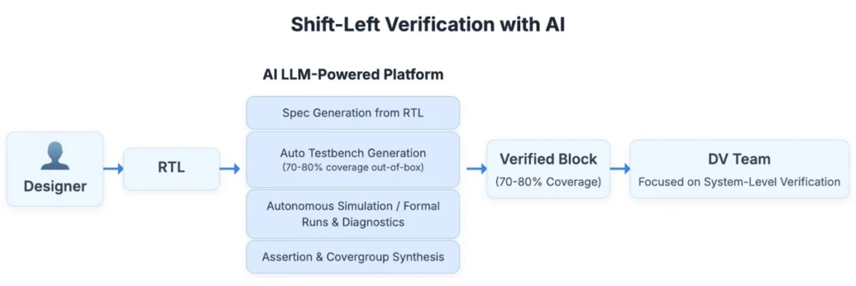
"Shift left" refers to the practice of moving verification tasks earlier in the development schedule. Historically, designers were reluctant to perform deep verification because of the steep learning curve associated with verification tools. Writing SystemVerilog Assertions (SVA) or setting up UVM environments requires expertise that differs significantly from writing synthesisable RTL.
AI assistants and LLM-powered platforms are now bridging this expertise gap. By utilizing natural language processing and pattern recognition, these tools can translate a designer’s intent into high-quality verification assets. This allows designers to verify individual blocks—the "units" of hardware—before they are ever handed off to the DV team.
The implications of this shift are profound. When designers verify their own blocks, they catch "shallow" bugs immediately. This ensures that when the DV team receives the code, they are testing a stable foundation, allowing them to focus on complex, system-level interactions and "corner-case" scenarios that involve multiple asynchronous clock domains or power-management states.
High-Fidelity Specifications as the Foundation
Every successful verification cycle begins with a clear specification, often referred to as the "mental model" of the design. Traditionally, specifications have been static documents—PDFs or spreadsheets—that are prone to becoming outdated as the design evolves. AI-based assistants are transforming these into "executable specifications."

By using LLMs to expand concise design outlines into structured specifications, teams can define functional behaviors, interface protocols, and boundary conditions with high precision. This automation ensures that the specification remains a "single source of truth." When the specification is version-controlled and machine-readable, AI tools can automatically generate the corresponding design and verification collateral. This "spec-first" approach minimizes ambiguities that typically lead to functional bugs, effectively cutting down on downstream debugging hours.
Automated Unit-Level Verification and Assertion Generation
Unit-level verification is the hardware equivalent of software unit testing. Industry data suggests that catching a bug at the block level is up to 100 times cheaper than catching it after the chip has been manufactured. Despite this, many designers skip rigorous block-level testing due to the manual labor involved in creating testbenches and drivers.
AI-driven tools are now capable of generating these unit tests automatically. A designer can provide the RTL code or a functional spec, and the AI can produce a complete test environment in minutes. For instance, verifying a complex First-In-First-Out (FIFO) buffer or a memory controller, which previously took days of manual testbench writing, can now reach high coverage levels in the time it takes for an engineer to take a coffee break.
Furthermore, AI is solving the "SVA problem." SystemVerilog Assertions are powerful tools for catching bugs at the source, but they are notoriously difficult to write correctly. AI assistants can now take a natural language description, such as "the grant signal must never be high if the request signal was not high in the previous cycle," and generate the mathematically correct SVA code. This allows assertions to be embedded throughout the RTL, providing immediate feedback during simulation.
Enhancing Functional Coverage Through Designer Insight
While code coverage measures which lines of code were executed, functional coverage measures whether specific logic scenarios were actually tested. Designers possess the best "tribal knowledge" regarding the edge cases of their specific blocks, yet they often lack the time to write the complex covergroups required to track these scenarios.
AI tools can bridge this gap by converting a designer’s natural-language insights into SystemVerilog covergroups. This ensures that the DV team has visibility into whether the most critical and risky scenarios have been exercised. By automating the syntax-heavy aspects of coverage, AI allows the human engineers to focus on the "what" rather than the "how."
Industry Reactions and Market Implications
The move toward AI-augmented verification has prompted significant investment from major EDA players. Executives at companies like Cadence and Synopsys have noted that the integration of AI is not merely a feature update but a fundamental re-architecture of the design flow. During recent industry symposiums, the consensus among CTOs has been that AI will be the primary driver in managing the complexity of 2nm nodes and beyond, where the number of possible states in a design exceeds the number of atoms in the known universe.
Market analysts suggest that organizations adopting AI-driven "shift left" methodologies will see a significant reduction in "non-recurring engineering" (NRE) costs. By reducing the number of required silicon respins—which can cost upwards of $10 million for advanced nodes—companies can maintain higher margins and more predictable release cycles.
The Future of the Verification Ecosystem
The ultimate goal of this evolution is a unified, AI-enhanced verification platform. In this future state, simulation, formal analysis, emulation, and debugging will not be siloed activities but interconnected processes sharing a common AI-driven data backend. Such a platform will not only automate routine tasks but will offer predictive analytics, suggesting which tests are most likely to find bugs or pinpointing the root cause of a failure by analyzing trillions of simulation cycles.
As the traditional "wall" between design and verification continues to erode, the roles of engineers will evolve. Verification engineers will transition from being "test writers" to "architects of verification strategy," focusing on system-level integrity and security. Designers, supported by AI, will become more self-sufficient, ensuring that quality is "baked in" from the first line of code.
In conclusion, the integration of AI into the semiconductor verification workflow is a necessary response to the overwhelming complexity of modern electronics. By enabling a "shift left" strategy, AI reduces the 70% effort burden currently hampering the industry. The result is a more efficient, predictable, and robust development cycle. As the industry moves forward, the divide will grow between those who leverage AI to accelerate their workflows and those who remain tethered to manual, high-latency methodologies. The future of silicon is not just about smaller transistors, but about smarter ways to ensure they work.