
The semiconductor industry is currently undergoing one of its most significant structural transitions since the invention of the integrated circuit. For design teams adopting three-dimensional integrated circuit (3D-IC) architectures, the relentless pursuit of performance and reliability brings a familiar, yet increasingly complex, set of challenges: managing power density, dissipating concentrated heat, and navigating the intricate dance of physics within stacked architectures. While 3D-ICs offer significant advantages in physical footprint, interconnect speed, power efficiency, and cost-per-function, they also introduce a level of complexity that traditional two-dimensional (2D) design methodologies are ill-equipped to handle. Successfully navigating these hurdles requires a sophisticated approach that leverages automated multiphysics analysis, enhanced cross-industry collaboration, and a strategic "shift-left" methodology.
The Escalating Stakes of 3D-IC Integration
The transition from traditional 2D system-on-chip (SoC) architectures to heterogeneous integration and full 3D stacking has fundamentally altered the semiconductor design landscape. In the 2D era, design teams relied heavily on well-established process design kits (PDKs) provided by foundries. These kits offered a predictable path to success because the physical interactions between components were largely restricted to a single plane. However, the move to 3D-ICs introduces novel materials, massive data volumes, and complex vertical interaction effects that cannot be easily modeled using legacy tools.
Designers can no longer afford to abstract away mechanical, thermal, and power phenomena as secondary concerns. In a 3D stack, these forces are central to achieving a reliable design. The fundamental relationship between power and heat is the primary driver of this complexity: power consumption directly generates thermal energy, and in a confined 3D space, this heat has fewer escape routes. This thermal buildup causes metal wires to expand and distort, while simultaneously altering the switching behavior of transistors. Such changes cascade through the design, necessitating updated power estimates and fresh timing analyses in a continuous loop.
The concept of a "known good die"—a staple of 2D manufacturing—is now evolving into the more stringent requirement of a "known good stack." In a vertically integrated system, a single failure in one layer can compromise the reliability and functionality of the entire system. This "multiphysics" interaction means that physical phenomena impact both the structural integrity and the electrical performance of the design. Without careful consideration, these effects can lead to catastrophic yield losses during manufacturing or, more concerningly, latent reliability problems that manifest only after the product is in the field.

A Chronology of Semiconductor Evolution: From Planar to 3D
To understand the current state of 3D-IC design, one must look at the chronological progression of the industry over the last decade.
- The Planar Era (Pre-2010s): Design focused on shrinking transistors on a single silicon plane. Thermal management was largely a package-level concern, and mechanical stress was rarely a factor in electrical timing.
- The Rise of FinFET and 2.5D (2010–2018): As planar scaling hit physical limits, the industry moved to FinFET transistors and 2.5D packaging (using silicon interposers). This introduced the first major need to manage heat across multiple chips on a single substrate.
- The 3D-IC Revolution (2019–Present): True 3D stacking, utilizing Through-Silicon Vias (TSVs) and hybrid bonding, became commercially viable for high-performance computing (HPC) and AI accelerators. This era necessitated the birth of multiphysics analysis, as the proximity of dies created unprecedented thermal and mechanical coupling.
As the industry moves toward 2025 and beyond, the complexity is expected to scale exponentially. Market data suggests that the 3D-IC market is poised for a compound annual growth rate (CAGR) exceeding 20%, driven by the demand for AI processing power that 2D architectures can no longer sustain due to the "memory wall" and power delivery constraints.
The Interplay of Physical Phenomena: Data and Technical Drivers
The technical challenges of 3D-ICs are best understood through the lens of four primary physical domains: electrical, thermal, mechanical, and power. These domains are no longer siloed; they are deeply interdependent.
Thermal and Power Dynamics
In a 3D stack, the middle dies are effectively insulated by the layers above and below them. Data shows that power densities in high-performance AI chips can now exceed 1W/mm², leading to localized hotspots that can reach temperatures well above the rated limits of the silicon. When a transistor heats up, its carrier mobility decreases, leading to slower switching speeds. If the design tools do not account for this localized heating, the final chip may fail to meet its timing targets, resulting in "timing closure" issues that are discovered only after the chip has been manufactured.
Mechanical Stress and Reliability
The materials used in 3D-ICs—silicon, copper pillars, glass substrates, and various polymers—all have different coefficients of thermal expansion (CTE). As the chip heats and cools during operation, these materials expand and contract at different rates. This creates mechanical stress that can lead to:

- Warpage: The entire package may bow, leading to solder joint failures.
- Delamination: Layers may peel apart under repeated thermal cycling.
- Micro-crack formation: Stress concentrations around TSVs can cause cracks that sever electrical connections.
Traditional concerns like electromigration (EM), electrical parasitics (PEX), voltage drop (IR), and electrostatic discharge (ESD) are now compounded by these newer thermal and mechanical interactions.
Collaboration and the Common Language of 3Dblox
Beyond the technical intricacies, successful 3D-IC projects hinge on close cooperation across a diverse ecosystem. This includes chip designers, package engineers, foundry partners, and outsourced semiconductor assembly and test (OSAT) companies. Historically, these groups operated in silos, using different tools and data formats.
To bridge this gap, the industry has moved toward standardization. The IEEE’s 3Dblox initiative is a critical development in this area. It provides a standardized way to represent 3D-IC structures, allowing different tools from various vendors to "speak" the same language. This interoperability is vital for protecting intellectual property (IP) while allowing foundries and OSATs to provide the necessary process data for accurate simulation. Tighter integration allows cross-functional teams to identify and address risks early in the design cycle, preventing the "wall-crossing" errors that often plague complex integration projects.
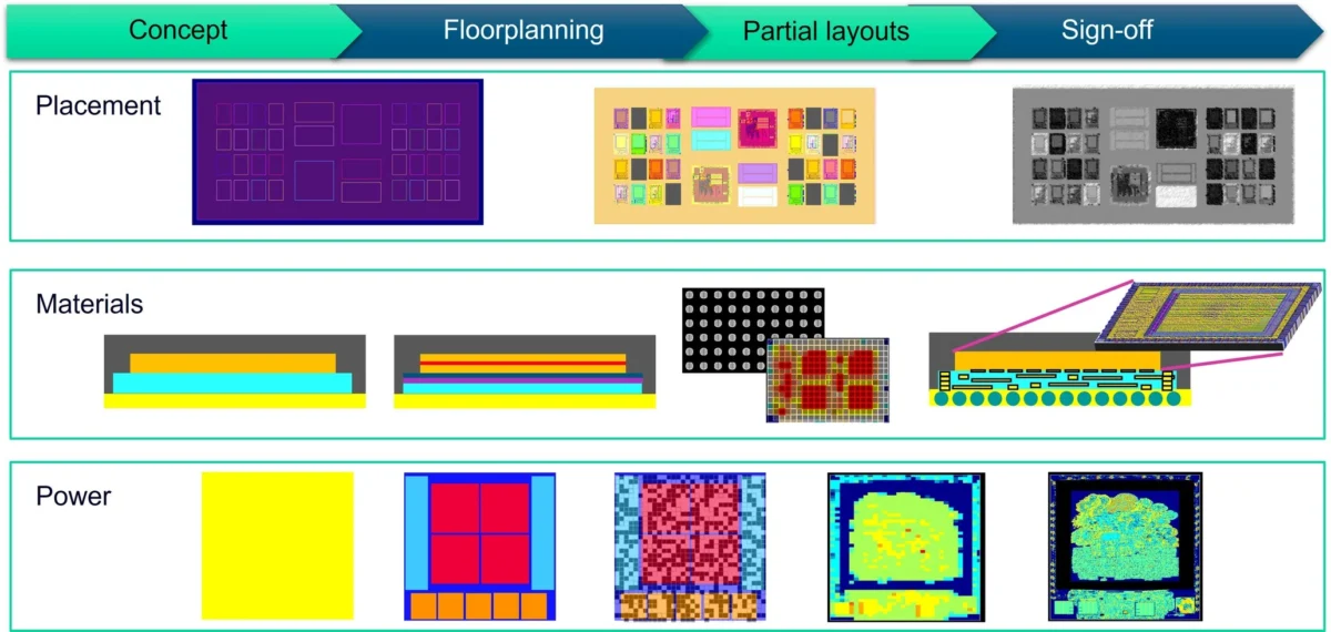
The Shift-Left Methodology: Simulation at the Conceptual Phase
The "shift-left" philosophy advocates for pushing analysis and decision-making to the earliest feasible point in the design process. For 3D-ICs, this means conducting "what-if" studies and simulating thermal stress long before the final layout is completed.
In the traditional "shift-right" or reactive model, thermal and mechanical analysis was performed at the very end of the design cycle as a final sign-off check. If a problem was found, it often required a complete redesign of the stack, leading to months of delays. In contrast, a shift-left approach allows designers to:

- Optimize Floorplanning: Move high-power logic units away from each other or away from heat-sensitive memory components early in the process.
- Material Selection: Evaluate the impact of different substrates (e.g., glass vs. silicon) on thermal dissipation before committing to a manufacturing path.
- Early Power Integrity: Simulate IR drop across multiple tiers to ensure stable power delivery to the top-most dies in the stack.
Modern tools, such as Siemens EDA’s Calibre 3DStress and Simcenter Flotherm, enable this early-stage analysis. By combining GDSII-level detail with advanced thermal solvers, these tools provide "push-button" results that highlight hotspots and stress regions within familiar design environments.
Official Responses and Industry Perspectives
Industry leaders at Siemens Digital Industries Software emphasize that the goal of these automated workflows is not to turn every IC designer into a thermal or mechanical expert. Instead, the objective is to democratize multiphysics insight.
John Ferguson and Sheltha Nolke of Siemens EDA have noted that the complexity of 3D-IC design is such that manual iteration is no longer humanly possible. The sheer volume of data—capturing wire, oxide, and transistor details across multiple dies—requires automation to deliver actionable insights. Their perspective is that the "Digital Twin" concept, which has been successful in aerospace and automotive industries, is now a necessity for semiconductor design. By creating a comprehensive digital twin of the 3D-IC, teams can simulate the entire manufacturing and operational lifecycle of the device before a single wafer is processed.
Foundries like TSMC and Samsung have also responded by integrating these multiphysics checks into their certified design flows. This ensures that when a designer uses an automated tool, the results are backed by the foundry’s own empirical data on material behavior and process variations.
Broader Impact and Future Implications
The move toward automated multiphysics and 3D-IC architectures has implications that extend far beyond the design lab. It is a fundamental enabler for the next generation of technological advancement.

The AI and High-Performance Computing Impact
The generative AI boom is entirely dependent on the bandwidth provided by HBM (High Bandwidth Memory) stacked on top of or alongside logic units. Without the multiphysics analysis described, the thermal throttling required to keep these chips from melting would render them no faster than previous generations.
Emerging Technologies: Photonics and Liquid Cooling
As 3D-ICs continue to push the limits of physics, we are seeing the emergence of even more radical solutions. Silicon photonics is being integrated into 3D stacks to allow for light-based signal delivery, which generates significantly less heat than traditional copper interconnects. Furthermore, research into chip-level liquid cooling—where microfluidic channels are etched directly into the silicon stack—is moving from the laboratory to high-end data center applications.
The Role of Artificial Intelligence in EDA
To address the steep learning curves associated with 3D-IC design, EDA vendors are increasingly integrating AI and machine learning into their platforms. These AI "agents" can help designers optimize die placement for thermal efficiency or automatically suggest dummy fill patterns to mitigate mechanical stress. This investment in AI-driven design tools aims to reduce the time-to-market for complex chips while maintaining high yields.
In conclusion, the transition to 3D-IC is not merely a change in packaging; it is a fundamental shift in how we approach the physics of computation. By embracing automated multiphysics analysis and a shift-left methodology, the semiconductor industry is building the foundation for a future where the constraints of 2D space no longer limit the potential of silicon innovation. The pursuit of the "known good stack" is a challenging journey, but with the right tools and collaborative frameworks, it is the path to the next era of electronic performance.