
In the high-stakes environment of modern semiconductor fabrication, the transition from theoretical design to physical silicon is fraught with escalating costs and shrinking timelines. As the industry pushes toward sub-5nm nodes, the complexity of three-dimensional structures like FinFETs (Fin Field-Effect Transistors) demands a level of precision that traditional trial-and-error methodologies can no longer provide. To address these challenges, engineers are increasingly turning to Virtual Design of Experiments (DOE) and predictive modeling to expose integration risks long before the first wafer enters the cleanroom. However, the efficacy of these virtual environments is entirely dependent on the accuracy of the underlying process models. Reliable prediction requires a rigorous correlation between model inputs and measurable physical outputs, necessitating a sophisticated approach to model calibration.
The Strategic Importance of Virtual Pathfinding
The semiconductor industry operates under the relentless pressure of Moore’s Law, where a delay of even a few weeks in product release can result in millions of dollars in lost revenue and a diminished market position. In this context, "pathfinding"—the phase where engineers determine the most viable manufacturing route for a new device—is critical. Traditionally, this involved running "short-loop" wafers through the fab to test various etch and deposition parameters. However, with the cost of advanced logic wafers exceeding $20,000 per start, the financial burden of physical experimentation has become prohibitive.

Virtual DOE offers a digital alternative, allowing for the simulation of thousands of process variations in a fraction of the time and cost required for physical trials. By utilizing platforms such as SEMulator3D, developed by Lam Research’s Semiverse Solutions, engineers can create "digital twins" of their fabrication processes. These models allow for the exploration of a vast parameter space, identifying potential yield-limiting defects and sensitivity issues early in the development cycle. Yet, for a digital twin to be useful, it must behave exactly like the equipment on the fab floor. This is where Process Model Calibration (PMC) and the identification of critical parameters become the linchpins of successful process integration.
Chronology of the Calibration and Integration Workflow
The integration of a new FinFET node typically follows a structured chronological progression, moving from structural definition to virtual validation and finally to physical manufacturing.
- Structural Definition and Target Extraction: The process begins with the physical measurement of existing silicon samples using Transmission Electron Microscopy (TEM). These high-resolution images provide the ground truth for the model. For a standard FinFET, this involves measuring the silicon fin’s height, width, and the profile of the Shallow Trench Isolation (STI) oxide.
- Initial Model Construction: A virtual process flow is built, replicating the deposition, lithography, and etching steps used in the fab. This includes defining the chemical and physical properties of the materials involved.
- Parameter Sensitivity Analysis: Engineers identify the myriad variables that could influence the final structure—ranging from plasma etch ratios to the angular distribution of ions.
- Virtual DOE and Monte Carlo Simulation: Thousands of simulations are run to understand how variations in these parameters affect the final critical dimensions (CD).
- Optimization and Alignment: Using regression analysis, the virtual model is "tuned" or calibrated until its outputs match the TEM measurements with sub-nanometer accuracy.
- Fab Implementation: The calibrated settings are used to inform the actual recipes used on the manufacturing equipment, significantly reducing the number of physical test wafers required.
Technical Deep Dive: Calibrating the FinFET Profile
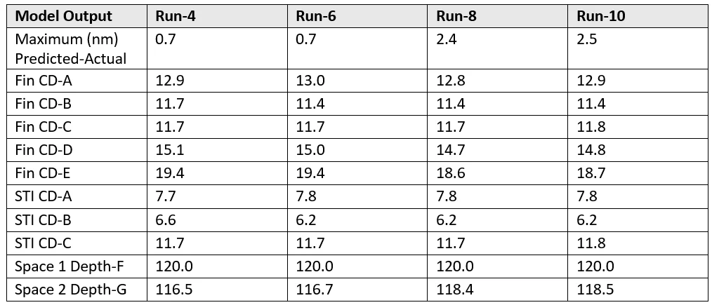
In a recent study conducted by Lam Research, the focus was placed on the STI etch sequence of a FinFET device, a critical step that defines the shape and performance of the transistor. The calibration targets were extracted from TEM-like cross-sections, focusing on dimensions both above and below the STI oxide. Measurements were taken at five distinct locations (labeled A through E) to capture the full geometry of the fin, including the top width, the slope of the sidewalls, and the total etch depth.

The modeling methodology utilized a looping deposition and etch sequence to simulate the complex interaction of plasma chemistry. A key challenge in this process is the "loading effect," where the density of the pattern influences the etch rate. In this experiment, the software accounted for polymer deposition factors that create thickness differences between narrow (inner) spaces and wider (outer) spaces. A thinner polymer passivation layer in the inner spaces results in increased silicon removal compared to outer spaces, a phenomenon that must be precisely modeled to avoid structural failures.
To achieve this, the team applied pattern loading multiplier factors at the start of the etch sequence. For instance, the etch ratio for the open mask was set to 1.0, while the dense array was set to 0.75. As the virtual etch proceeded, the inner spaces gradually became deeper than the outer spaces due to these deposition differentials. The final simulated over-etch depths reached 120 nm for inner spaces and 116 nm for outer spaces, closely mimicking observed fab behavior.
Data-Driven Insights: Identifying Key Parameters
One of the primary hurdles in process modeling is the sheer volume of variables. In the FinFET study, engineers initially identified 33 model variables that could potentially influence the profile. Managing such a large variable set is computationally expensive and analytically complex.

To streamline the process, the "Identify Important Parameters" (IIP) feature of the SEMulator3D Analytics suite was employed. Through 1,000 Monte Carlo simulation runs under a uniform distribution, the software performed a sensitivity analysis to rank the variables by their impact on the final profile. This analysis successfully narrowed the field from 33 variables to the 10 most critical factors. These included:
- Lateral to vertical etch ratios.
- Angular distribution of source particles.
- Polymer deposition thickness and uniformity.
- Pattern loading multipliers for isolated vs. dense regions.
- Ion-enhanced etch components.
By focusing only on these 10 parameters, the team could execute a more targeted virtual DOE for profile calibration. This involved an additional 2,000 Monte Carlo simulations to establish strong correlations between the top (location A) and bottom (location E) fin CDs and the primary model factors.
Results: Achieving Sub-Nanometer Precision
The ultimate goal of the calibration exercise was to minimize the deviation between the virtual model’s measurements and the actual wafer-based target metrology. The SEMulator3D Analytics PMC package utilized linear regression calibration, fitted to the Monte Carlo data, to optimize the process parameters.

The results of this calibration were highly successful. Over ten different calibration trials using random starting points, the system converged on optimized values that provided an exceptional fit to the physical data. In the best-performing trial (Run-4), the maximum deviation from the target metrology was reduced to just 0.7 nm. Across all successful trials, the highest deviation ranged from 0.7 nm to 2.5 nm. In the context of a semiconductor feature that may only be 10-20 nm wide, achieving sub-nanometer accuracy is essential for ensuring that the simulation can reliably predict electrical performance and yield.
Industry Implications and Economic Impact
The shift toward highly calibrated virtual models has profound implications for the semiconductor industry’s economic and environmental footprint. From a financial perspective, the ability to replace physical "DOE wafers" with virtual simulations represents a massive cost saving. For a leading-edge logic company, reducing the R&D cycle by just one month can be worth hundreds of millions of dollars in "first-to-market" advantage.
Furthermore, there is a significant sustainability benefit. Semiconductor manufacturing is resource-intensive, requiring vast amounts of ultra-pure water, electricity, and specialized chemicals. By reducing the number of physical test wafers required to calibrate a process, companies can lower their chemical waste and carbon footprint, aligning with broader industry goals for "Green Fab" operations.

Industry analysts suggest that the integration of AI and machine learning into these calibration tools will be the next frontier. As manufacturing equipment becomes more "sensor-rich," real-time data from the fab could be fed back into the virtual model, allowing for continuous, automated calibration. This would create a closed-loop system where the digital twin evolves in tandem with the physical equipment, further tightening the window of process variability.
Conclusion
As the semiconductor industry navigates the complexities of the angstrom era, the reliance on advanced analytics and virtual modeling will only grow. The study demonstrated by Brett Lowe and the team at Lam Research underscores that the value of predictive modeling is unlocked only through rigorous calibration. By reducing 33 complex variables to 10 manageable factors and achieving sub-nanometer alignment with physical reality, SEMulator3D Analytics has proven that virtual pathfinding is no longer a luxury, but a necessity. This methodology not only accelerates the release of next-generation FinFET and Gate-All-Around (GAA) devices but also establishes a new standard for precision in the digital age of manufacturing. Through the synergy of TEM metrology, Monte Carlo simulations, and automated regression, the path from design to high-volume manufacturing has never been clearer or more efficient.