
The PCI-SIG, the consortium responsible for the peripheral component interconnect express (PCIe) standard, has officially set the stage for the next decade of high-speed data transfer with the announcement of the PCIe 8.0 specification. Targeting a raw data rate of 256 gigatransfers per second (GT/s) per lane, the new standard is engineered to provide up to 1 terabyte per second (TB/s) of aggregate bidirectional bandwidth in a traditional x16 configuration. This development represents a significant leap in interconnect technology, arriving at a time when artificial intelligence (AI), machine learning (ML), and high-performance computing (HPC) are pushing existing hardware architectures to their absolute physical and logical limits. As data-intensive workloads become the norm in hyperscale data centers, the transition to PCIe 8.0 is viewed not merely as an incremental speed boost, but as a critical architectural inflection point for the global semiconductor industry.
The Evolutionary Trajectory of PCI Express
The journey to PCIe 8.0 is defined by a consistent, disciplined cadence of performance doubling. Since its inception, the PCI-SIG has maintained a roadmap that roughly doubles the bandwidth of the specification every three years, ensuring that system architects have a predictable path for I/O scaling. To understand the magnitude of PCIe 8.0, one must look at the rapid progression of the standard over the last decade.
The release of PCIe 4.0 in 2017 provided 16 GT/s per lane, followed relatively quickly by PCIe 5.0 in 2019, which doubled that to 32 GT/s. The introduction of PCIe 6.0 in 2022 marked a major technical shift, as the industry moved from Non-Return-to-Zero (NRZ) signaling to Pulse Amplitude Modulation 4-level (PAM4) signaling, alongside the introduction of Flow Control Unit (Flit) based encoding and Forward Error Correction (FEC). PCIe 7.0, currently in the final stages of its lifecycle toward full adoption, targets 128 GT/s.
With PCIe 8.0, the target of 256 GT/s ensures that the standard remains the dominant interconnect for internal system communications. This trajectory is essential for maintaining backward compatibility, a hallmark of the PCIe ecosystem that allows legacy hardware to operate within newer systems, thereby protecting billions of dollars in existing infrastructure investment. By preserving the familiar software and programming models, the PCI-SIG ensures that the transition to 256 GT/s does not require a fundamental rewrite of operating system kernels or device drivers, focusing instead on the physical and link layer challenges of moving data at near-light speeds.
Technical Specifications and Performance Metrics
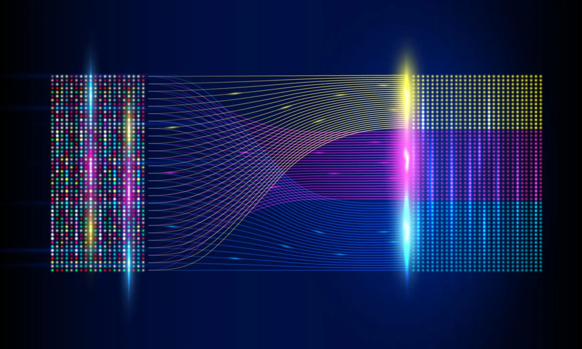
The headline figure for PCIe 8.0 is its 256 GT/s per lane throughput. In a standard x16 slot, commonly used for high-end graphics processing units (GPUs) and AI accelerators, this translates to 512 GB/s in a single direction or 1 TB/s of total bidirectional bandwidth. This level of throughput is necessary to feed the massive computational appetites of modern neural networks, which often require hundreds of gigabytes of parameters to be swapped between memory and processing cores in milliseconds.
The technical shift required to achieve these speeds involves significant advancements in the Physical Layer (PHY) and the Controller IP. At 256 GT/s, signal integrity becomes the primary concern. The industry is currently exploring how to maintain the PAM4 signaling utilized in PCIe 6.0 and 7.0 or whether further modulation refinements will be necessary. Regardless of the specific modulation, the "unit interval"—the time allowed for a single bit to be transmitted—becomes incredibly small, leaving almost no margin for electrical noise, jitter, or signal attenuation.
Furthermore, PCIe 8.0 will place unprecedented demands on flow control and protocol efficiency. As the data rate increases, the overhead associated with packet headers and error correction must be minimized to ensure that the "effective" bandwidth remains as close to the "theoretical" bandwidth as possible. This requires highly scalable controller architectures capable of handling massive transaction volumes without introducing latency bottlenecks.
The Catalyst: AI, HPC, and Hyperscale Demands
The primary driver for the accelerated development of PCIe 8.0 is the explosive growth of the AI market. Modern AI training clusters, such as those utilized for Large Language Models (LLMs), rely on a "scale-up" and "scale-out" architecture. In a scale-up scenario, multiple GPUs within a single server must communicate with each other and with the central processing unit (CPU) at extreme speeds to synchronize gradients and share memory resources.
Currently, data movement is often the bottleneck in these systems. While compute power (measured in FLOPS) has increased exponentially, the ability to move data between the processor and the memory hierarchy has lagged. PCIe 8.0 aims to bridge this "memory wall" by providing the fat pipes necessary for high-speed I/O.
Beyond the server box, PCIe 8.0 is also being designed with disaggregated computing in mind. In a disaggregated data center, resources like storage, memory, and compute are pooled and interconnected via high-speed fabrics. PCIe, along with the Compute Express Link (CXL) protocol which runs on the PCIe physical layer, is the foundational technology enabling this transition. By providing 256 GT/s, PCIe 8.0 allows for the creation of massive, low-latency fabrics that can span across multiple racks, enabling a more efficient utilization of hardware resources.
Hardware Design Challenges and the Shift to Optical Interconnects
As speeds reach 256 GT/s, traditional copper traces on printed circuit boards (PCBs) face severe physical limitations. Signal loss increases dramatically with frequency, meaning that the distance a signal can travel over standard copper (the "reach") shrinks with every generation. For PCIe 8.0, maintaining a usable reach on standard PCB materials like FR4 is virtually impossible, necessitating the use of ultra-low-loss materials or the integration of "retimers"—specialized chips that clean up and re-amplify the signal.
To address these reach challenges, the industry is increasingly looking toward PCIe over optics. The PCI-SIG has already begun developing specifications to support optical signaling, which would allow PCIe links to extend several meters rather than just a few inches. This transition is expected to be a major component of the PCIe 8.0 era. Optical interconnects offer the advantage of near-zero signal degradation over distance and immunity to electromagnetic interference, though they introduce new challenges in terms of cost, power consumption, and the complexity of laser integration.
For System-on-Chip (SoC) designers, the integration of PCIe 8.0 IP involves navigating complex thermal and power envelopes. High-speed PHYs are power-hungry components, and at 256 GT/s, managing the heat generated by I/O subsystems becomes a critical part of the design cycle. Companies like Rambus are currently developing controller and PHY IP that prioritize "performance with confidence," focusing on robust link management and recovery mechanisms that can handle the inevitable errors that occur at such high frequencies.
Industry Reactions and Ecosystem Readiness
The announcement of PCIe 8.0 has been met with broad support from the semiconductor ecosystem, including major players like Intel, AMD, NVIDIA, and ARM. While these companies are currently focused on deploying PCIe 5.0 and 6.0 products, the long lead times associated with chip design—often three to five years—mean that planning for PCIe 8.0 must begin immediately.
Analysts suggest that the first PCIe 8.0-compliant silicon will likely appear in the late 2020s, targeting the "AI-first" data centers of the 2030s. "The cadence of the PCI-SIG is vital for our roadmap planning," noted one senior architect at a leading GPU firm. "Knowing that we have a path to 1 TB/s allows us to design next-generation accelerators with the confidence that the system bus won’t be the primary bottleneck."
IP providers are also playing a crucial role in this transition. By providing pre-validated PCIe 8.0 controller and PHY designs, companies like Rambus enable SoC designers to mitigate the risks associated with such a high-speed transition. This "ecosystem readiness" is essential for the rapid adoption of the standard once the final specification is ratified.
Broader Implications and Future Outlook
The implications of PCIe 8.0 extend far beyond faster gaming PCs or quicker file transfers. This technology is a foundational pillar for the next era of global digital infrastructure. By enabling more efficient AI training and inference, PCIe 8.0 will indirectly contribute to advancements in fields ranging from drug discovery and climate modeling to autonomous systems and real-time global financial analytics.
Furthermore, the standard reinforces the trend toward "open" interconnects. By providing a high-performance, royalty-free standard, the PCI-SIG prevents the fragmentation of the hardware market into proprietary, vendor-locked ecosystems. This ensures that a GPU from one vendor can work seamlessly with a CPU from another, fostering competition and innovation across the entire industry.
As the industry looks toward the 2030s, the focus will shift to how PCIe 8.0 integrates with other emerging technologies. The synergy between PCIe 8.0 and CXL 4.0 (or 5.0) will be particularly important, as it will define how coherent memory sharing is handled at the terabyte-per-second level. Additionally, the move toward "chiplets"—where a single processor is made of multiple smaller dies—will rely on PCIe-like high-speed interfaces to maintain performance across the package.
In conclusion, the PCIe 8.0 specification is a bold statement of intent from the PCI-SIG. It acknowledges that the data demands of the future are not just growing, but accelerating. By targeting 256 GT/s, the standard provides the roadmap necessary for the semiconductor industry to continue its march toward more powerful, efficient, and interconnected computing systems. For architects and designers, the work begins now to solve the formidable signal integrity and power challenges that come with the 1 TB/s era, ensuring that the next generation of SoCs is ready for the workloads of tomorrow.