
When discussing high-performance memory at Samsung, the spotlight invariably falls on High Bandwidth Memory (HBM) and the expansive infrastructure powering artificial intelligence. This focus, while critical for data centers and AI accelerators, often overshadows advancements that directly impact consumer electronics, particularly smartphones. A Galaxy smartphone, by design and necessity, will not integrate HBM in the same manner as a data center GPU; the specific requirements for power consumption, thermal management, and physical footprint in mobile devices make direct HBM integration impractical. However, the sophisticated learnings derived from pushing the boundaries of HBM development — spanning material science, advanced packaging, and rigorous quality control protocols — are far from confined to the server room. These insights are increasingly being distilled and applied to technologies much closer to the everyday user, a strategic pivot exemplified by Samsung’s significant new investment in femtosecond laser processing.
This latest initiative from Samsung centers on pioneering laser cutting and processing technology engineered to operate at an extraordinarily fine scale. The ambition is to achieve unparalleled precision in the manufacturing and quality assurance of its semiconductor chips. The true value proposition for mobile devices does not lie in a hypothetical HBM-equipped Galaxy, but rather in how profound improvements in memory processing and packaging techniques can ultimately elevate the performance and longevity of components integral to every smartphone, such as NAND flash storage modules and various elements within the System-on-Chip (SoC).
Beyond the Hype: Subtlety in Semiconductor Evolution
For the end-user, this class of advancement will not manifest as a bold, new specification on a product sheet or a flashy marketing slogan. Instead, its impact will be experienced through the subtle yet profound improvements in the device’s operational lifespan. Imagine internal memory that maintains its speed and reliability over years of use, a noticeable reduction in performance variability between individual chips, or critical components that demonstrate enhanced resilience against the inevitable wear and tear of daily operation. In essence, while it may not offer the immediate, marketable appeal of a higher megapixel camera or a faster processor core count, it represents a foundational improvement—one of those critical, behind-the-scenes innovations that fundamentally enhance the real-world user experience and device sustainability.
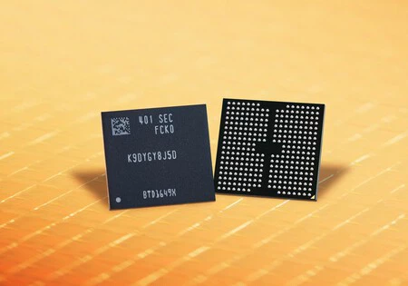
NAND flash memory is a prime candidate to benefit from these advancements, remaining a critical, non-negotiable component in every modern smartphone. Its role extends from hosting the operating system and applications to securely storing all user data, photos, and videos. Samsung’s intensified focus on memory and storage innovation is not coincidental; it arrives amidst growing industrial pressure and a soaring demand, particularly from the AI sector, which has catalyzed a significant surge in memory prices across the board. This market dynamic underscores the urgency for manufacturers like Samsung to refine their production processes, ensuring both efficiency and quality in a highly competitive and volatile landscape.
The Precision of Femtosecond Lasers: A Technical Deep Dive
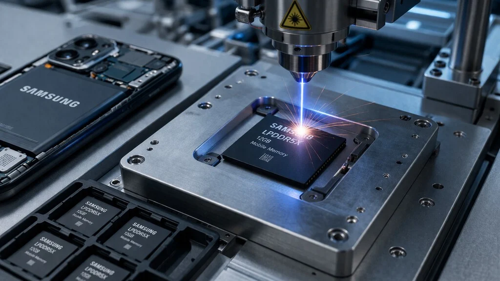
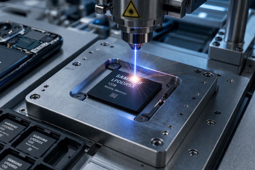
The core technology driving this new Samsung initiative is a femtosecond laser cutting system. To grasp its significance, one must understand the scale at which it operates. A femtosecond is an incredibly brief unit of time, one millionth of a billionth of a second (10⁻¹⁵ seconds). When a laser emits pulses of light at such ultrashort durations, it interacts with material in a fundamentally different way than traditional, longer-pulse lasers. This phenomenon is often referred to as "cold ablation."
In conventional laser processing, longer pulses (nanosecond or picosecond range) deliver energy over a relatively extended period, causing the material to heat up significantly before it vaporizes or melts. This heat can spread to the surrounding material, creating a "heat-affected zone" (HAZ) where micro-cracks, material stresses, and unwanted debris can form. These imperfections are detrimental in semiconductor manufacturing, where features are measured in nanometers.
Femtosecond lasers, conversely, deliver immense energy in an extremely short burst. This allows the laser energy to be absorbed by the material so rapidly that the chemical bonds break before the surrounding material has time to heat up substantially. The material essentially vaporizes instantaneously from the surface without melting or causing significant thermal damage to adjacent areas. This results in:
- Exceptional Precision: The ability to create incredibly fine cuts and features with minimal collateral damage, down to micron and sub-micron levels.
- Reduced Heat-Affected Zone (HAZ): Significantly less thermal stress on the surrounding material, preserving its structural integrity, which is vital for delicate semiconductor structures.
- Minimized Debris and Micro-cracking: Cleaner cuts lead to fewer particles and structural weaknesses, crucial for long-term reliability and preventing electrical shorts.
- Versatility: Capable of processing a wider range of materials, including delicate and complex semiconductor substrates like silicon, glass, and various polymers, with superior results compared to mechanical methods.
This technology represents a paradigm shift from traditional methods, such as mechanical dicing saws, which physically cut wafers and can introduce vibrations, chipping, and require coolant, further complicating the process. By adopting femtosecond laser technology, Samsung aims to achieve unparalleled levels of precision, which directly translates into higher manufacturing yields, reduced defects, and ultimately, more reliable and durable chips.
Strategic Implications for Samsung’s Semiconductor Business
This move aligns perfectly with a broader trend observed across many Samsung products: significant improvements are not always unveiled as visible features on launch day. Often, they manifest as meticulously refined internal components—parts that are more precisely manufactured, more energy-efficient, or inherently less prone to degradation over time. This foundational approach underscores a commitment to quality that goes beyond superficial marketing.
For its semiconductor business, a sector where margins are razor-thin and competition is fierce, such an improvement in manufacturing precision and efficiency is transformative. It may not alter the headline specifications of a chip, but it can profoundly influence its long-term reliability, performance consistency, and overall lifespan. In the context of the intensely competitive semiconductor market, where every nanometer and every percentage point of yield matters, the ability to produce chips with greater consistency and fewer defects offers a substantial competitive advantage. This strategic investment positions Samsung against rivals like SK Hynix, Micron, and TSMC by enabling higher quality output and potentially reducing manufacturing costs over time.
Should this advanced laser processing be broadly applied to high-volume components like NAND flash modules or general-purpose system chips, the discernible effect for the end-user will primarily be an enhanced long-term stability rather than a groundbreaking, day-one feature. This inference is well-grounded in Samsung’s industrial logic regarding memory production and advanced manufacturing processes, focusing on sustainable performance and reliability.
The Critical Role of NAND in the Mobile Ecosystem
NAND flash memory is the backbone of digital storage in virtually all consumer electronics, from smartphones and tablets to solid-state drives (SSDs) in computers. In a smartphone, NAND flash stores everything from the operating system and pre-installed applications to user-generated content like photos, videos, and documents. The performance, endurance, and cost of NAND directly influence the overall user experience and the final price point of mobile devices.
The architecture of NAND flash involves stacking multiple layers of memory cells vertically (3D NAND) to achieve higher densities and capacities. As the number of layers increases (Samsung is already at its 9th generation V-NAND, pushing towards 1,000 layers), the challenges in manufacturing precision become exponentially more complex. Aligning these layers perfectly, ensuring uniform cell characteristics, and minimizing defects throughout the intricate vertical structure are monumental tasks. Femtosecond laser technology can be instrumental here, enabling more precise etching, cutting, and shaping of the complex 3D structures, which can lead to:
- Higher Density and Capacity: More precise manufacturing allows for denser stacking of layers and smaller cell sizes without compromising integrity, leading to higher storage capacities in the same physical footprint, crucial for modern smartphones.
- Improved Endurance: Reduced manufacturing defects and thermal stress can lead to more robust memory cells, enhancing their ability to withstand repeated read/write cycles over the device’s lifespan. This is critical for preventing performance degradation and data loss, a common issue in aging devices.
- Enhanced Performance: More uniform and pristine cell structures can contribute to faster read and write speeds, ensuring applications launch quicker and data transfers are more efficient throughout the device’s life, contributing to a consistently fluid user experience.
- Better Yields and Lower Costs: By minimizing defects during the manufacturing process, Samsung can produce more usable chips per wafer, directly impacting production costs and, potentially, mitigating the impact of rising raw material and market-driven price increases.
Market Dynamics and the AI Influence on Memory Pricing
The current market landscape further accentuates the importance of such manufacturing innovations. The explosion of generative AI has created an unprecedented demand for high-performance memory, particularly HBM, which is optimized for the massive parallel processing required by AI models. This surging demand has, in turn, put upward pressure on the prices of other memory types, including DRAM and NAND flash, as manufacturing capacities are stretched and raw material costs escalate. Reports indicate significant price increases, with some memory types seeing hikes of over 180% in recent periods.
While mobile devices don’t use HBM directly, the overall increase in memory prices due to AI indirectly affects the cost of smartphone components. By improving manufacturing efficiency and yield through technologies like femtosecond lasers, Samsung can better manage its production costs for NAND and other mobile-centric chips. This strategic move helps Samsung maintain its competitive edge as a leading memory supplier and mitigates some of the external cost pressures that could otherwise translate into higher prices for consumers or reduced profit margins for the company. It also supports Samsung’s overarching goal of providing stable component pricing to its mobile division, ensuring competitiveness in the smartphone market.
Broader Impact and Future Outlook for Samsung’s Semiconductor Strategy
Samsung’s adoption of femtosecond laser technology extends beyond mobile, representing a significant stride in its overall semiconductor manufacturing capabilities. This advanced processing method is applicable across various segments, including automotive chips, IoT devices, and even general-purpose computing. The consistent theme is the pursuit of foundational improvements that enhance reliability, efficiency, and longevity across its entire chip portfolio.
While there is no immediate announcement of a Galaxy device explicitly marketing this technology, its integration will likely be gradual and pervasive. The benefits will accrue over time, subtly elevating the quality and performance baseline of future Samsung products. This approach underscores Samsung’s long-term vision: to sustain its leadership not merely by pushing raw power specifications but by fundamentally enhancing how it engineers and manufactures the core components that underpin all its innovations. This reflects a shift towards deep engineering and process innovation as a key differentiator.
This strategic investment positions Samsung to tackle several critical challenges in the modern semiconductor industry:
- Miniaturization: As chips continue to shrink and transistor densities increase, the need for ultra-precise manufacturing methods becomes paramount. Femtosecond lasers provide the necessary control at the atomic level, enabling the creation of intricate circuitry without thermal damage.
- Advanced Packaging: Techniques like chip stacking and 3D integration require incredibly accurate cutting and drilling to create Through-Silicon Vias (TSVs) and other interconnects. Cold ablation minimizes damage to these delicate structures, facilitating more complex and efficient packaging solutions.
- Heterogeneous Integration: Combining different types of chips (e.g., logic, memory, sensors) into a single package demands precise handling and processing of diverse materials, a strength of femtosecond lasers. This is crucial for creating highly integrated, power-efficient modules for future devices.
- Supply Chain Resilience: By improving in-house manufacturing capabilities and efficiency, Samsung strengthens its control over its supply chain, a crucial factor in an era of global semiconductor shortages and geopolitical complexities. This reduces reliance on external vendors for critical process steps.
- Environmental Impact: The precision and clean nature of femtosecond laser processing can also contribute to more environmentally friendly manufacturing by reducing waste material and the need for harsh chemicals often associated with traditional etching processes.
The adoption of such advanced laser technology is not unique to Samsung; the semiconductor industry as a whole is exploring and implementing similar high-precision manufacturing tools. However, Samsung’s explicit focus on applying these high-end learnings from HBM and AI infrastructure to mainstream mobile components demonstrates a holistic strategy for technological dominance. It signifies a move towards making every chip, regardless of its end application, as robust and efficient as possible from its very inception. This proactive investment underlines Samsung’s commitment to maintaining its position as a global leader in semiconductor technology, anticipating future demands for performance, reliability, and sustainability.
In conclusion, Samsung’s strategic embrace of femtosecond laser technology is a testament to its commitment to foundational engineering excellence. It represents an evolution in how technological advancements translate from cutting-edge research to tangible consumer benefits. While not a flashy marketing point, this precision manufacturing leap promises a future where mobile devices are not just more powerful, but also significantly more durable, consistent, and reliable over their entire lifespan, ultimately delivering a superior and more sustainable user experience.
Source: etnews.
Images: Dall-E with editing, Samsung.