
The global semiconductor ecosystem is currently navigating a period of intense technological acceleration and geopolitical recalibration, marked by significant leaps in hardware verification, power electronics, and artificial intelligence infrastructure. Recent developments from industry leaders such as Intel, Siemens, and Nvidia, alongside critical research from top-tier academic institutions, suggest a shift toward more integrated, secure, and power-efficient computing architectures. At the same time, the industry faces mounting pressures from talent poaching in Asia and fluctuating revenues in Europe, forcing a reevaluation of supply chain stability and intellectual property protection.
The Verification Breakthrough: Accelerating Time-to-Market
One of the most significant technical milestones this quarter comes from a collaboration between Siemens and Nvidia. The two companies have announced a verification breakthrough that allows for the capture of tens of trillions of verification cycles within just a few days. This feat was achieved by integrating Siemens’ Veloce proFPGA CS hardware architecture with Nvidia’s performance-optimized chip designs.
In the traditional semiconductor design cycle, verification often consumes up to 70% of the total development time. As System-on-Chip (SoC) complexity grows—driven by the demands of generative AI and autonomous driving—the ability to run trillions of cycles rapidly is no longer a luxury but a necessity. By leveraging scalable hardware-assisted verification, designers can identify "corner case" bugs that might otherwise remain hidden until the post-silicon phase, where corrections are exponentially more expensive. This collaboration signals a new era in electronic design automation (EDA), where the bottleneck of simulation speed is being systematically dismantled through hardware-software co-design.
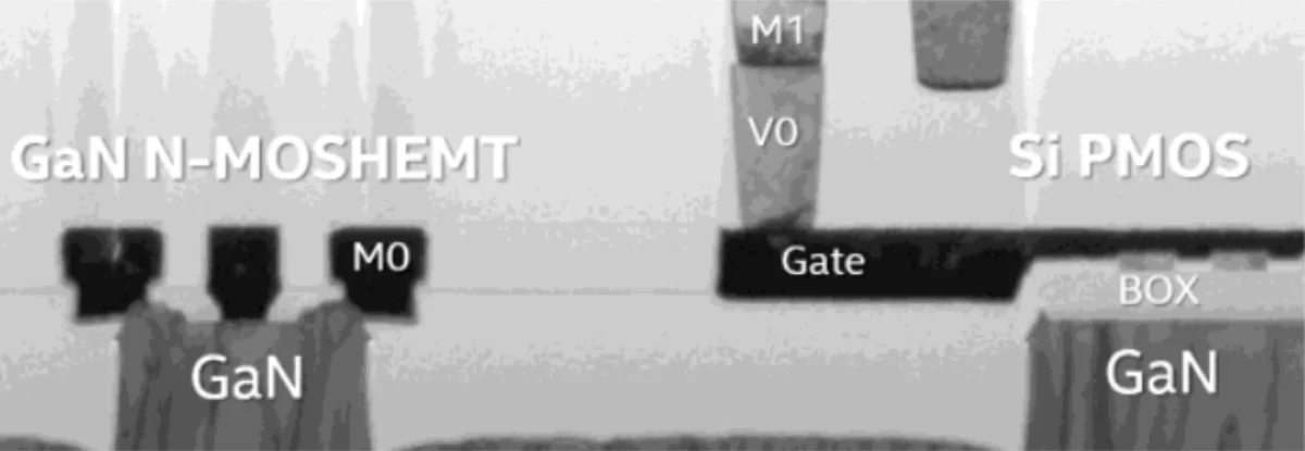
Intel and the Rise of GaN-on-Silicon
Intel Foundry has recently showcased a major advancement in power electronics: the development of the thinnest Gallium Nitride (GaN) chiplet integrated alongside silicon logic. Specifically, Intel demonstrated a cross-sectional view of a GaN power transistor and a silicon logic transistor built side-by-side on the same 300 mm GaN-on-silicon wafer.
The transition to 300 mm wafers for GaN is a pivotal move for the industry. GaN is highly prized for its high-voltage capabilities and superior thermal efficiency compared to traditional silicon, making it ideal for power delivery in data centers and electric vehicles (EVs). However, GaN has historically been restricted to smaller wafer sizes, which limits economies of scale. Intel’s ability to manufacture GaN on 300 mm silicon substrates suggests that high-performance power management can now be integrated directly into the logic manufacturing process. This integration reduces parasitic inductance, saves space, and significantly improves the power-to-performance ratio of next-generation processors.

Geopolitical Friction and the Global Talent War
While technical milestones continue to be reached, the geopolitical landscape remains volatile. In Taiwan, the epicenter of global foundry capacity, the domestic integrated circuit (IC) industry has issued a formal call for the establishment of strategic stockpiles. This move is seen as a defensive measure against potential supply chain disruptions, whether caused by natural disasters, such as the frequent seismic activity in the region, or escalating cross-strait tensions.
Simultaneously, the industry is grappling with an aggressive talent war. Reports indicate that mainland China has intensified its efforts to poach high-level engineering talent from Taiwan. This "brain drain" is particularly concerning for the development of advanced process nodes and specialized memory technologies. Despite legislative efforts in Taiwan to protect "national core technologies," the lure of high compensation and leadership roles in China’s domestic chip projects remains a persistent challenge for Taiwanese firms like TSMC and MediaTek.
In Europe, the outlook is more tempered. Recent financial reports indicate a revenue drop across several key semiconductor segments. Analysts attribute this decline to a slowdown in industrial automation and a cooling of the European automotive sector, which has traditionally been a stronghold for the region’s chipmakers. This downturn highlights the vulnerability of the European market to shifting global demand and the slower-than-expected adoption of certain green technologies.
AI Infrastructure: Alibaba and Meta’s Next Moves
The race for AI supremacy continues to drive massive infrastructure investments. Alibaba has recently launched a 10,000-card computing cluster designed specifically for high-performance AI training and inference. This massive deployment is intended to provide the raw computational power required for the next generation of Large Language Models (LLMs) and represents China’s determination to remain competitive despite U.S.-led export restrictions on high-end GPUs.
On the software and modeling side, Meta has debuted "Muse Spark," a natively multimodal reasoning model. Unlike previous models that often required separate "wrappers" to handle different types of data, Muse Spark is designed from the ground up to support tool-use, visual chains of thought, and multi-agent orchestration. This development points toward a future where AI agents can autonomously navigate complex tasks across different media types, further increasing the demand for specialized AI accelerators and high-bandwidth memory (HBM).
Advanced Packaging: The HBM Bottleneck
The surge in AI demand has made High Bandwidth Memory (HBM) one of the most critical components in the data center. Hanmi Semiconductor has announced plans to release its second-generation hybrid bonder for HBM this year. Hybrid bonding is a technique that allows for the vertical stacking of memory dies without the use of traditional solder bumps, resulting in much higher interconnect density and better thermal performance.

As HBM moves toward HBM4 and beyond, the precision required in packaging is becoming as challenging as the lithography used for the chips themselves. The industry is watching Hanmi’s release closely, as it could determine which memory manufacturers—SK Hynix, Samsung, or Micron—gain the upper hand in the high-stakes AI memory market.
Security Threats: GPU Rowhammer and Silent Data Corruption
As hardware becomes more complex, new security vulnerabilities are emerging. Researchers have identified a "GPU Rowhammer" attack, an evolution of the classic DRAM exploit. By repeatedly accessing certain memory rows, attackers can induce bit-flips in adjacent rows, potentially gaining unauthorized access or corrupting sensitive data. The extension of this vulnerability to GPUs is particularly alarming given the central role GPUs play in cloud computing and AI.
In tandem with these active attacks, the industry is fighting "Silent Data Corruption" (SDC). SDC occurs when a processor or memory unit produces an incorrect result without triggering an error flag. Noam Brousard, VP at proteanTecs, has highlighted that as transistors shrink, environmental factors and aging can lead to these unpredictable errors. The solution lies in "deep data" monitoring—placing on-chip sensors that can detect degradation before it leads to a system-level failure.
Furthermore, there is a growing global effort to combat the grey market and counterfeit chips. Stakeholders are advocating for a certificate-based, tamper-proof tagging system that is permanent and immutable. Such a system would ensure that critical infrastructure—from power grids to medical devices—uses only verified, authentic components.
Automotive Evolution: BMW’s Hydrogen Bet and Japan’s Struggles
The automotive sector is witnessing a divergence in strategy. While most of the industry is focused on battery-electric vehicles (BEVs), BMW continues to invest in hydrogen power. The German automaker argues that hydrogen fuel cells offer a viable alternative for long-range transport and for regions where charging infrastructure is insufficient.
Meanwhile, the Japanese automotive industry is facing significant headwinds. Traditionally dominant in the internal combustion engine (ICE) and hybrid markets, Japanese firms have been slower to transition to full electrification compared to their Chinese and American counterparts. This delay, coupled with supply chain fragilities, has led to a period of restructuring and strategic reassessment within the Japanese automotive supply chain.

Academic Contributions: AI-Driven Materials Science
Research institutions continue to push the boundaries of what is possible at the nanoscale. Cornell University researchers have developed an agentic AI architecture capable of converting electron microscopy images into full materials analysis in minutes—a process that previously took days or weeks of manual labor.
At UC San Diego, engineers have designed a new piezoelectric resonator-based DC-DC converter. This chip design could drastically improve power management in data centers by increasing the efficiency of how GPUs manage electricity, reducing heat waste and operational costs. Similarly, the University of Michigan has introduced a hardware-software co-design for "Compute-In-Memory" (CIM) architectures, specifically optimized for running AI on edge devices with minimal power consumption.
Conclusion and Outlook
The semiconductor industry is currently at a crossroads where the demands of artificial intelligence are forcing a rapid evolution in hardware design, manufacturing, and security. The breakthroughs in 300 mm GaN wafers and ultra-fast verification cycles suggest that the industry is rising to the challenge of building more powerful and efficient systems. However, the shadow of geopolitical instability and the persistent threat of hardware-level security flaws remain significant hurdles.
As the industry moves into the second half of 2026, the focus will likely remain on securing talent, stabilizing supply chains through strategic stockpiling, and refining the advanced packaging techniques necessary to keep pace with the AI revolution. The upcoming series of global summits, including the TSMC Technology Symposium and the MRS Spring Meeting, will serve as critical venues for the industry to align on these pressing technical and economic challenges.