
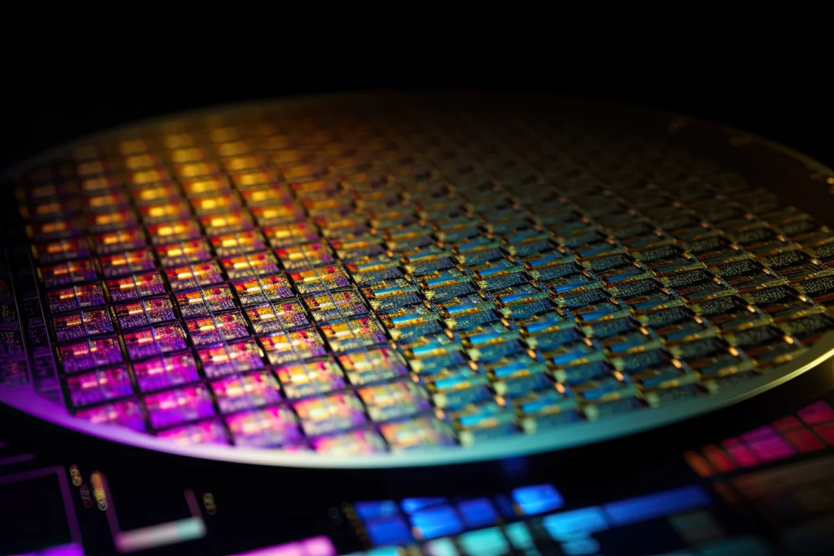
The semiconductor industry has reached a pivotal juncture where the traditional benchmark of achieving "first silicon" is no longer the sole indicator of a technology’s readiness for the commercial market. As artificial intelligence (AI) and high-performance computing (HPC) systems scale at an unprecedented rate, the underlying hardware must undergo rigorous, system-level validation long before mass production begins. In a significant move to de-risk the next generation of compute-intensive platforms, Synopsys has announced the successful silicon validation of the world’s first High-Bandwidth Memory 4 (HBM4) IP test chip. This milestone, achieved through successful linking with HBM4 memory devices, represents a critical step in overcoming the "memory wall" that currently limits the throughput of advanced AI accelerators and data center processors.
The Critical Shift in Memory Architecture and Validation
For decades, the primary focus of semiconductor advancement was the scaling of logic gates and the increase of clock speeds. However, the rise of Large Language Models (LLMs) and massive data analytics has shifted the bottleneck from pure processing power to memory bandwidth. High-Bandwidth Memory (HBM) emerged as the industry’s solution, utilizing vertically stacked DRAM dies connected via through-silicon vias (TSVs) to provide a wide interface and high data rates in a compact footprint.
The transition from HBM3 and HBM3E to HBM4 marks the most significant architectural shift in the history of the standard. Unlike previous generations, HBM4 doubles the interface width from 1,024 bits to 2,048 bits per stack. This doubling of the "highway" for data requires a complete overhaul of the physical layer (PHY), the memory controller, and the packaging technologies used to integrate these components. Because the physical margins for error—timing, voltage, and thermal—have shrunk to near-zero, the industry has had to move away from sequential validation. The Synopsys HBM4 IP test chip validation proves that the ecosystem is moving toward a parallel development model where logic IP and memory silicon are tested in tandem within a representative system environment.
Chronology of HBM Evolution and the Path to HBM4
The road to HBM4 has been defined by a rapid acceleration in data transfer requirements. To understand the significance of the current milestone, one must look at the trajectory of the technology over the last decade:
- HBM1 (2013): Introduced the concept of 3D-stacked memory with a 1,024-bit interface, offering roughly 128 GB/s of bandwidth. It was primarily adopted in high-end enthusiast GPUs.
- HBM2/2E (2016-2018): Increased the pin speed and density, pushing bandwidth toward 256–307 GB/s per stack. This generation saw widespread adoption in professional visualization and early AI research.
- HBM3 (2022): Represented a major leap, with speeds reaching 6.4 Gbps per pin and total bandwidth exceeding 819 GB/s. This became the standard for the first wave of generative AI hardware.
- HBM3E (2023-2024): An evolutionary refinement that pushed pin speeds to 8.0–9.2 Gbps, supporting the massive demand of NVIDIA’s Blackwell and Hopper architectures.
- HBM4 (2025-2026 Roadmap): The current frontier. By moving to a 2,048-bit interface, HBM4 aims to provide more than 1.5 TB/s of bandwidth per stack while maintaining or improving power efficiency.
The Synopsys validation event serves as a bridge between the HBM3E era and the full-scale deployment of HBM4. By demonstrating a functional link between logic IP and HBM4 memory at this stage, Synopsys has provided the industry with a blueprint for the 2,048-bit transition, which is expected to enter high-volume manufacturing in late 2025 or early 2026.
Technical Data and Performance Benchmarks
The recent validation of the Synopsys HBM4 IP test chip yielded specific data points that underscore the technical feasibility of the new standard. The most notable metric is the achievement of a 9.2 Gbps data rate per pin. While this matches the upper limits of HBM3E, it is achieved over the much wider 2,048-bit HBM4 interface, effectively doubling the total throughput compared to existing solutions.
Key technical observations from the silicon validation include:
- Signal Integrity and Eye Openings: At 9.2 Gbps, the electrical signals are highly susceptible to noise. Synopsys reported "clean eye openings," a technical term indicating that the PHY can clearly distinguish between binary high and low signals despite the presence of jitter and crosstalk.
- Scalability: While the current test utilized 9.2 Gbps DRAMs, the Synopsys HBM4 IP is architected to support significantly higher speeds as the memory devices themselves mature. Future iterations are expected to reach 12 Gbps or higher, targeting a total bandwidth of nearly 2 TB/s per stack.
- Power and Thermal Margins: Because HBM4 stacks are expected to be taller (up to 16-high stacks), managing the heat generated by the memory-logic interface is critical. The test chip validation included monitoring power noise and thermal stability, ensuring that the denser interconnects do not lead to localized overheating.
The integration of the PHY and controller in this test chip allows designers to see how the system handles the physical realities of advanced packaging, such as Chip-on-Wafer-on-Substrate (CoWoS) and other interposer technologies.
Ecosystem Alignment and Strategic Responses
The success of HBM4 is not the achievement of a single company but rather a collaborative effort involving IP providers, foundries, and memory vendors. The validation of the Synopsys IP requires close alignment with major memory manufacturers—SK Hynix, Samsung, and Micron—as well as leading foundries like TSMC.

Industry analysts suggest that the "successful link-up" mentioned by Synopsys implies a high degree of interoperability between the logic IP and the actual memory silicon produced by these vendors. While official statements from memory manufacturers remain focused on their internal production yields, the availability of silicon-proven IP from a provider like Synopsys acts as a catalyst. It allows system-on-chip (SoC) designers to begin their HBM4-based designs with the confidence that the communication layer between the processor and the memory is already functional.
Foundry partners have also reacted positively to these developments. As the industry moves toward 2nm and 3nm process nodes, the physical distance between the logic and the memory becomes a critical design variable. The validation of the HBM4 interface path provides foundries with the necessary data to optimize their advanced packaging recipes, ensuring that the interposers can handle the increased routing density of the 2,048-bit bus.
Analyzing the Challenges: Crosstalk and Timing Uncertainty
Despite the success of the test chip, the path to HBM4 mass adoption is fraught with engineering hurdles. The increase to a 2,048-bit interface means that the number of physical connections (microbumps) between the memory stack and the logic die has increased dramatically. This density introduces two primary risks: crosstalk and timing uncertainty.
Crosstalk occurs when the electrical signal on one wire interferes with the signal on an adjacent wire. With 2,048 signals firing at nearly 10 billion times per second in a confined space, the electromagnetic interference is substantial. Synopsys addressed this through sophisticated signaling strategies and PHY architecture designed to cancel out noise.
Timing uncertainty, or jitter, is the other major hurdle. In a synchronous system, all 2,048 bits of data must arrive at the controller at precisely the right moment to be read correctly. Even a microscopic variation in the length of the traces on the silicon interposer can cause data to arrive out of sync. The validation of the HBM4 IP indicates that the adaptive calibration techniques built into the Synopsys controller are capable of compensating for these physical variations in real-time.
Broader Impact on AI and HPC Markets
The implications of early HBM4 validation extend far beyond the laboratory. For developers of AI accelerators—companies like NVIDIA, AMD, and various hyperscale cloud providers—this milestone reduces the "integration risk" that has plagued multi-die designs.
In the current market, the lead time for a flagship AI chip can exceed 18 months. If a design team were to wait for HBM4 memory to be commercially available in bulk before testing their logic interface, they would risk a catastrophic failure or a multi-quarter delay if the two components failed to communicate properly. By using silicon-proven IP, these teams can move forward with their architectural decisions, knowing that the most complex part of the interface—the HBM4 PHY—has already been validated in a real-world silicon environment.
Furthermore, HBM4 is expected to enable a new class of "Base Die" configurations. In some HBM4 implementations, the bottom layer of the memory stack (the base die) may be manufactured on a logic process rather than a traditional DRAM process. This allows for even tighter integration between the memory and the processor, potentially including custom logic within the memory stack itself. Synopsys’ early validation provides the foundation for exploring these advanced "custom HBM" architectures.
Conclusion: The Roadmap Toward Production
The validation of the world’s first HBM4 IP test chip by Synopsys marks the beginning of a new era in high-performance system design. It confirms that the technical specifications of the HBM4 standard are not just theoretical goals but are achievable in physical silicon. As the industry moves toward 2025, the focus will shift from initial validation to yield optimization and cost reduction.
For the AI and HPC sectors, the message is clear: the bandwidth constraints that have threatened to slow the progress of machine learning models are being addressed through aggressive innovation in memory interfaces. While HBM4 introduces unprecedented complexity in packaging and signal integrity, the availability of silicon-proven implementations ensures that the ecosystem is ready for the next wave of compute-intensive applications. The success of this test chip is a vital signal to system architects that the transition to 2,048-bit memory interfaces is well underway, paving the way for the next generation of supercomputing and generative AI.