
The global semiconductor industry is currently navigating a pivotal transition as the rapid evolution of Artificial Intelligence (AI) outpaces the physical and architectural limits of traditional monolithic compute systems. As trillion-parameter large language models (LLMs) become the standard for generative AI, the industry is shifting toward a systemic architecture where massive, distributed clusters of Graphics Processing Units (GPUs) and AI accelerators function as a single, unified computational engine. Central to this transformation is the emergence of Co-Packaged Optics (CPO), a technology designed to resolve the interconnect bottlenecks that threaten to stall AI progress. While CPO offers a path toward unprecedented bandwidth and energy efficiency, its integration requires overcoming significant engineering hurdles in assembly, alignment, and testing.
The Architectural Shift: From Monolithic to Distributed AI Clusters
The demand for computational power has grown exponentially since the debut of modern transformer-based models. Traditional server architectures, which relied on localized processing and standard copper-based interconnects, are no longer sufficient to handle the data movement required for synchronized training across thousands of nodes. This has led to the rise of two distinct scaling strategies within AI data center infrastructure: Scale-Up and Scale-Out.
Scale-Up refers to the internal communication within a single server rack or a localized cluster of accelerators. In this layer, GPUs communicate via high-speed proprietary or open-standard fabrics, such as NVIDIA’s NVLink or AMD’s Infinity Fabric. Historically, these connections relied on copper cables. However, as speeds exceed 200G per lane, the physical limitations of copper—specifically signal attenuation and heat generation—have become prohibitive.
Scale-Out involves the networking between different racks and across the broader data center, typically utilizing Ethernet or InfiniBand protocols. While Scale-Out networks have already begun adopting CPO switches to mitigate signal loss over longer distances, the next critical evolutionary step is the integration of Silicon Photonics into the Scale-Up layer. This integration is essential to transcend the bandwidth-distance limitations that currently restrict the physical size and efficiency of GPU clusters.
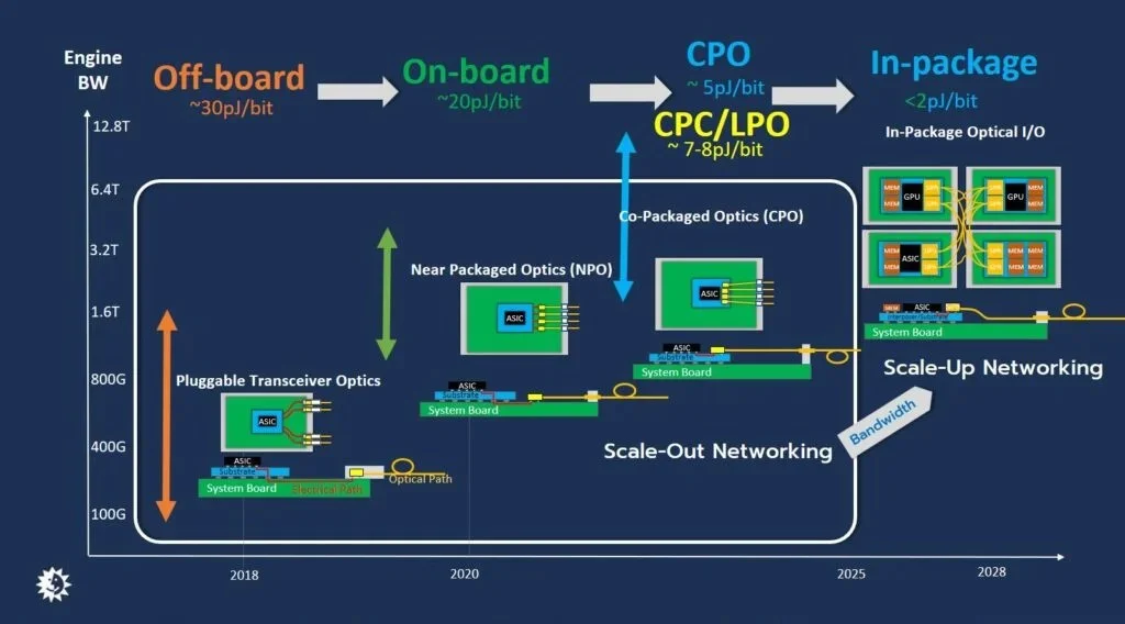
A Chronology of Optical Integration: 2018 to the Present
The journey toward CPO began in earnest around 2018 with the commercialization of silicon photonics-based pluggable optical transceivers. These modules allowed data centers to replace traditional electrical signals with light, significantly increasing reach. However, as data rates climbed from 400G to 800G and toward 1.6T, the "front-panel" approach—where transceivers are plugged into the faceplate of a switch—hit a wall. The electrical path between the switch ASIC and the front panel became a major source of power consumption and signal degradation.
To address this, the industry introduced Near Packaged Optics (NPO), which moved the optical engines (OEs) closer to the ASIC on the system board. The current cutting-edge frontier is Co-Packaged Optics, where the optical engine is integrated directly into the same package as the ASIC or GPU. This progression represents a 64-fold increase in bandwidth density over the last five years, coupled with a fivefold improvement in energy efficiency.

By shortening the electrical traces to the absolute minimum, CPO reduces the energy required to move a single bit of data. While conventional pluggable transceivers operate at approximately 20 to 30 picojoules (pJ) per bit, CPO implementations are targeting less than 5 pJ/bit. This shift is not merely a performance upgrade; it is a thermal necessity for data centers that are increasingly constrained by power delivery and cooling capacities.
Comparative Analysis of Interconnect Solutions
To understand the necessity of CPO, it is helpful to examine the current landscape of optical solutions and their respective performance metrics.
| Solution Type | Energy Efficiency | Bandwidth Capability | Typical Application |
|---|---|---|---|
| Conventional Pluggables | 20-30 pJ/bit | Up to 800G | Standard Data Center Networking |
| On-Board Optics (NPO) | ~20 pJ/bit | Up to 1.6T | High-Speed Switching |
| Co-Packaged Optics (CPO) | <5 pJ/bit | 3.2T – 6.4T | Next-Gen AI Scale-Up/Scale-Out |
The data indicates that while pluggable modules are reaching their ceiling at 800G or 1.6T, CPO is the only viable path to achieving the 3.2T to 6.4T bandwidths required for the next generation of AI accelerators.
Addressing the Bandwidth Density Mismatch
Despite the theoretical advantages of CPO, mass production is hindered by a critical disparity between the edge bandwidth density of AI chiplets and current optical interconnects. Modern AI chiplets, utilizing standards like Universal Chiplet Interconnect Express (UCIe) or the Optical Internetworking Forum (OIF) standards, can achieve an edge bandwidth density of approximately 3 terabits per second per millimeter (Tbps/mm).
In contrast, current state-of-the-art CPO solutions only achieve about 0.5 Tbps/mm. This six-fold gap means that the physical footprint of the optical interface is too large to match the processing power of the silicon it serves. Solving this requires the development of Photonic Integrated Circuits (PICs) with significantly smaller form factors and more compact Fiber Array Units (FAUs).
Current fiber pitches—the distance between individual optical fibers—often exceed 100 microns. Reducing this pitch while maintaining signal integrity is a major engineering challenge. Technologies such as Wavelength Division Multiplexing (WDM) and Dense Wavelength Division Multiplexing (DWDM) are being employed to increase the data-carrying capacity of each fiber, thereby reducing the total fiber count. However, these technologies introduce their own complexities, particularly the need for extreme wavelength stability across a wide range of operating temperatures.
Complexities in Assembly and Heterogeneous Integration
The assembly of a CPO module is one of the most complex tasks in modern semiconductor packaging. It requires the integration of lasers, optics, FAUs, and silicon integrated circuits across various wafer nodes. Two primary architectural approaches have emerged: Photonic FOPoP and Photonic 3D.

Photonic FOPoP (Fan-Out Package-on-Package) involves positioning the PIC on top of the Electronic Integrated Circuit (EIC). This method uses wafer-level fan-out processes and copper pillars to provide vertical connectivity. While effective for certain applications, it faces limitations in heat dissipation and vertical scaling.
Photonic 3D packaging is increasingly viewed as the preferred approach for high-performance AI applications. In this configuration, the PIC is placed at the bottom, and Through-Silicon Vias (TSVs) are used to connect to the top-mounted EIC. This allows for superior thermal management, as the heat-generating EIC is closer to the cooling solution. Furthermore, Photonic 3D supports data transmission rates exceeding 200G per lane, which is essential for the 3.2T and 6.4T engines currently under development.
The Challenge of Optical Alignment and Coupling
Precision is the primary hurdle in the physical assembly of CPO. While silicon wafers can be manufactured with nanometer precision, the mechanical components of optical systems—such as fibers and connectors—often have much wider tolerances.
Traditionally, the industry has relied on Active Alignment (AA). This process involves passing light through the components during assembly and using real-time feedback to find the position that optimizes optical coupling. Once the "sweet spot" is found, the components are permanently bonded with epoxy. However, this creates a "reliability trap." If a single fiber in a 64-fiber array fails or is damaged during installation, the entire multi-thousand-dollar CPO module must be scrapped because it cannot be repaired.
To address this, there is a significant industry push toward detachable FAU solutions. These would allow fibers to be plugged into the CPO module much like a standard cable. However, achieving sub-micron alignment accuracy in a detachable format—and maintaining that accuracy across multiple mating cycles—is a daunting task. One promising solution involves wafer-level optical couplers that expand the size of the laser beam at the interface, thereby increasing the tolerance for slight misalignments and enabling more scalable high-volume manufacturing (HVM).
Ensuring Yield through Known-Good Optical Engines (KGOE)
In a complex heterogeneous assembly, the cost of failure is high. If a faulty optical engine is integrated with a high-value GPU, the entire package is lost. This has necessitated the development of "Known-Good Optical Engines" (KGOE) through rigorous pre-assembly testing.
The preferred methodology for this is double-side wafer-level testing. This involves interfacing with one side of the wafer using Automatic Test Equipment (ATE) to check electrical functions, while simultaneously using detachable optical sockets on the other side to test photonic performance.

However, this testing regime presents mechanical challenges. In Photonic 3D configurations, the PICs are often thinned to below 100 microns to facilitate TSV performance. These ultra-thin wafers must withstand the significant mechanical pressure of ATE probes and optical sockets, which can reach the kilogram range. Packaging specialists like ASE are currently developing reinforced structures to protect these delicate components during the testing phase, ensuring that only functional engines proceed to final assembly.
Broader Impact and the Path Forward
The successful scaling of CPO technology will have profound implications for the global AI landscape. Beyond the performance gains, the transition to CPO is a critical component of the "Green AI" movement. By slashing the energy consumption of data movement, CPO helps mitigate the environmental impact of massive data centers.
Industry experts suggest that the widespread adoption of CPO will require unprecedented collaboration across the semiconductor ecosystem. Designers of EICs and PICs must work in tandem with packaging specialists and system integrators to ensure that every component—from the laser source to the fiber connector—is optimized for a unified architecture.
As companies like ASE and other leaders in the Outsourced Semiconductor Assembly and Test (OSAT) sector refine 3D packaging and testing protocols, the "bandwidth wall" that currently threatens AI scaling will likely begin to recede. The transition from pluggable optics to fully integrated co-packaged solutions marks the beginning of a new era in computational efficiency, providing the foundation upon which the next generation of artificial intelligence will be built. The focus now shifts from "if" CPO will be adopted to "how quickly" the industry can resolve the remaining manufacturing and alignment challenges to meet the insatiable demand for AI compute.