
Static Random Access Memory (SRAM) remains a fundamental pillar of modern computing, serving as the high-speed bridge between the processing core and the vast, slower expanses of external storage. However, as the semiconductor industry pushes into the sub-3nm era, a critical divergence has emerged: while logic transistors continue to shrink, SRAM cells have hit a physical and economic plateau. This stagnation has revitalized the "memory wall"—a term coined decades ago to describe the growing performance gap between processors and memory—threatening the efficiency of everything from mobile microcontrollers to the massive GPU clusters powering generative artificial intelligence.
A Decades-Old Prophecy Realized
The concept of the memory wall is not a new phenomenon. In 1990, John Hennessy and David Patterson, in their seminal work Computer Architecture: A Quantitative Approach, warned that memory latency and bandwidth would eventually become the primary bottlenecks for computing performance. For nearly thirty years, hardware architects successfully navigated this challenge by implementing complex hierarchies of cache. By using SRAM as a small, ultra-fast on-chip buffer (L1, L2, and L3 caches) backed by larger off-chip Dynamic Random Access Memory (DRAM), designers created the illusion of a memory system that was both massive and instantaneous.
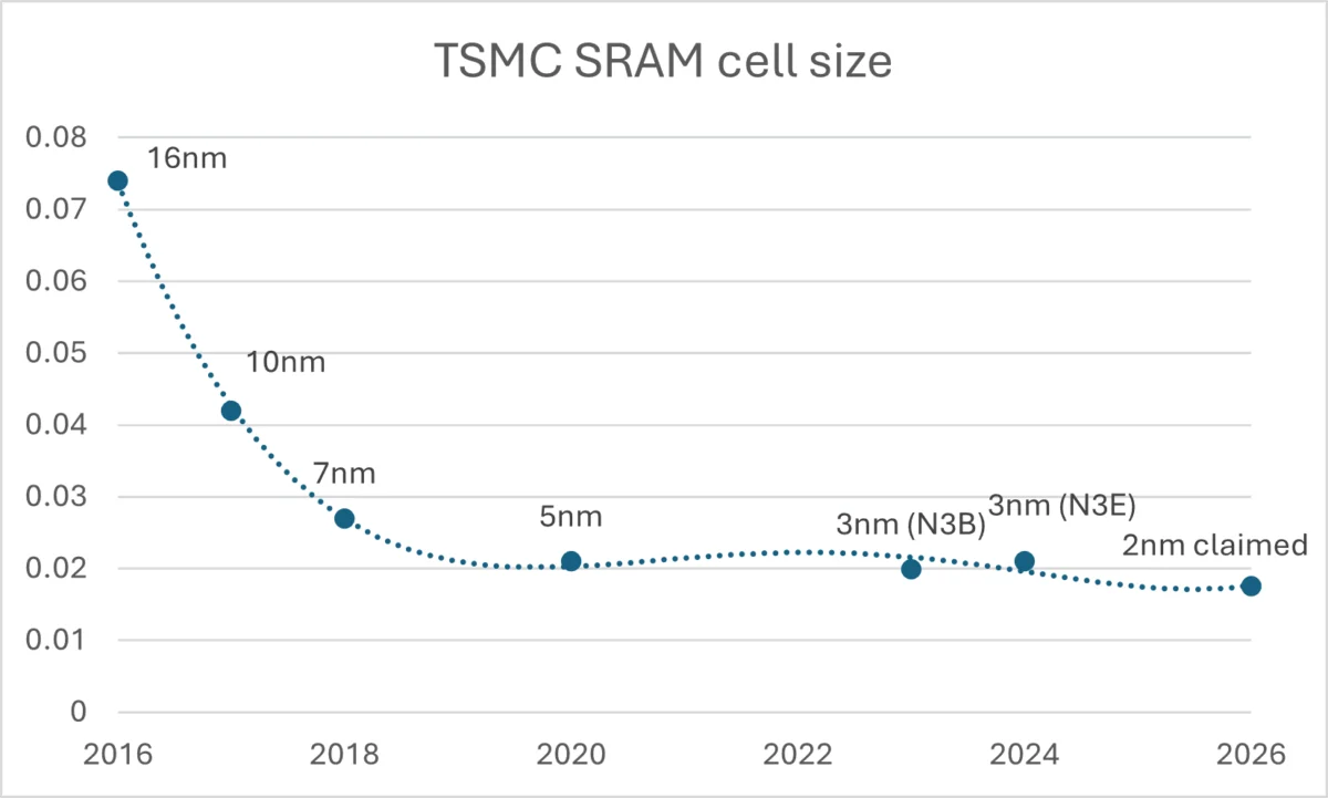
Chronologically, the industry enjoyed a "golden era" of scaling from the 65nm node down to the 5nm node. During this period, node transitions typically yielded density improvements between 50% and 100%. A chip designer could expect that moving to a smaller process would naturally shrink the footprint of both logic and memory, allowing for more cache on the same die area. However, as the industry transitioned to 3nm and now prepares for 2nm, that relationship has fractured. Current data suggests that SRAM bitcell scaling on leading-edge 2nm technologies has plummeted to less than 15% density improvement, representing a near-halt in the traditional Moore’s Law trajectory for memory.
The Physics of Stagnation: Why SRAM Won’t Shrink
The primary vehicle for on-chip memory is the 6-transistor (6T) bitcell. This architecture was designed for density, but it possesses an inherent physical conflict: the transistors responsible for accessing the data must compete with those responsible for storing it. As geometries shrink to the atomic level, process variations—tiny differences in how transistors are manufactured—become a significant percentage of the bitcell’s characteristics.
Industry experts, including Daryl Seitzer of Synopsys, note that the battle between read and write requirements in these tiny cells has reached a breaking point. In the 2nm regime, electrostatic control and random variation dominate the design. Furthermore, while logic scaling benefits from new transistor architectures like Gate-All-Around (GAA) nanosheets, SRAM speed has plateaued. This is largely due to the fact that wire resistance and bitline capacitance are increasing as dimensions narrow, while the supply voltage (Vdd) has remained stubbornly high to maintain stability.

The result is a widening "area tax." Because logic continues to shrink while SRAM does not, memory occupies an increasingly large percentage of the total silicon die. For many modern System-on-Chips (SoCs), SRAM now accounts for 50% or more of the die area. As chips approach the "reticle limit"—the maximum physical size a chip can be manufactured—designers are forced to choose between reducing the number of processing cores or cutting back on the cache, the latter of which forces the chip to rely on external memory that is orders of magnitude slower.
The AI Catalyst and the Bandwidth Gap
The rise of artificial intelligence has exacerbated the memory wall crisis. AI workloads, particularly Large Language Models (LLMs), require massive amounts of data to be moved constantly between memory and the processor. Ramin Farjadrad, CEO of Eliyan, points out a startling disparity: while processor performance has increased by nearly five orders of magnitude over the last two decades, memory bandwidth has grown by less than 100x. This 1,000x delta means that in many high-end AI applications, the processor is utilized only 20% of the time, spending the remaining 80% idling while waiting for data to arrive from memory.
In the context of LLM inference, the "KV-cache" (Key-Value cache) has become a notorious bottleneck. As model context lengths grow, the bandwidth required to access these cached values dominates performance. When compute improvements can no longer compensate for slow memory scaling, the burden shifts to software. Developers are now forced to optimize for data locality, quantization, and sparsity—techniques designed to minimize the amount of data that needs to be moved—rather than focusing purely on algorithmic complexity.
Foundry Responses and the 2nm Transition
Taiwan Semiconductor Manufacturing Company (TSMC), the world’s leading foundry, has acknowledged the difficulties of SRAM scaling but remains publicly optimistic about its upcoming 2nm nanosheet technology. TSMC claims that the transition to GAA transistors will provide better electrostatic control, potentially reducing leakage and improving the read/write behavior of memory cells.
However, many in the design community remain skeptical. Historically, the actual density gains achieved in mass production have often fallen short of early foundry projections. Rahul Thukral of Synopsys notes that much of the recent "memory area" improvements haven’t actually come from the memory bitcells themselves, but rather from shrinking the peripheral logic—the decoders and control circuitry—that surrounds the memory array. While this provides a temporary reprieve, it does not solve the fundamental problem of the non-scaling 6T bitcell.
Strategic Shifts: 3D Stacking and Disaggregation
Faced with the reality that SRAM may never scale efficiently again, the industry is pivoting toward radical architectural changes. One of the most promising solutions is the disaggregation of memory through chiplets and 3D stacking.

Under this model, designers place only the most critical Level 1 and Level 2 caches on the expensive, leading-edge 2nm logic die. The larger Level 3 or Level 4 caches are then moved to a separate "memory chiplet" manufactured on an older, more cost-effective process node (such as 7nm or 5nm). This memory chiplet is then bonded to the logic die using advanced packaging techniques like TSMC’s SoIC (System on Integrated Chips).
This approach allows for massive amounts of SRAM to be integrated without consuming precious real estate on the primary logic die. We are already seeing this in the High Bandwidth Memory (HBM) market, where stacks of DRAM are placed in the same package as GPUs. The next evolution, according to industry leaders at Cadence and Eliyan, involves using logic-optimized processes for the base die of these memory stacks, allowing for even higher bandwidth and potentially doubling the memory capacity accessible to the processor.
The Rise of Alternative Memories: MRAM and ReRAM
While SRAM is unlikely to be replaced entirely in high-speed L1/L2 caches, emerging memory technologies are gaining a foothold in other areas. Magnetoresistive RAM (MRAM) is increasingly seen as a viable successor to embedded flash and certain SRAM applications due to its high endurance and low leakage. Similarly, Resistive RAM (ReRAM) is finding adoption in microcontrollers and edge AI accelerators where non-volatile storage and low cost are prioritized over raw speed.
Nandan Nayampally of Baya Systems suggests that the industry is reaching an "architectural inflection point." The traditional model of a giant compute engine pulling data from a nearby memory pool is being challenged by "near-memory compute" and "in-memory compute" architectures. These designs distribute processing power directly into the memory array, reducing the distance data must travel and effectively bypassing the memory wall for specific workloads.
Conclusion: A New Era of Architectural Efficiency
The memory wall is no longer a theoretical hurdle; it is a defining constraint of the semiconductor industry. As SRAM scaling stalls, the era of "free" performance gains through node shrinks has ended. The future of computing will be defined by how efficiently designers can manage data movement rather than how many transistors they can cram into a logic gate.
This shift will require a holistic effort across the stack. Foundries must continue to innovate with new transistor structures; architects must embrace 3D stacking and chiplet disaggregation; and software engineers must write code that is fundamentally "memory-aware." While there is no "silver bullet" to solve the SRAM scaling crisis, the industry’s pivot toward architectural efficiency suggests that the memory wall, while higher than ever, may yet be overcome through ingenuity rather than raw scaling. As the industry moves toward rack-scale computing and unified resources, the ability to divide and manage memory effectively will remain the ultimate arbiter of performance.