
In the contemporary semiconductor landscape, global attention is frequently monopolized by high-bandwidth memory (HBM), massive graphics processing units (GPUs), and the sophisticated logic chips that power artificial intelligence. However, an equally significant transformation is occurring within the realm of specialty devices. These components, often described as the "unsung heroes" of the digital age, serve as the critical interface between the physical world and digital processing. Found in everything from the smartphone in a user’s pocket to the advanced power systems of electric vehicles (EVs) and the high-speed optical interconnects of data centers, specialty devices are experiencing a surge in demand and technical complexity that is reshaping the manufacturing sector.
As consumer electronics incorporate more sophisticated features with each successive generation, the industry is witnessing a pivot toward larger wafer sizes and more intricate materials. This transition is not merely a matter of scaling production; it represents a fundamental shift in how devices such as Micro-Electromechanical Systems (MEMS), CMOS Image Sensors (CIS), Silicon Carbide (SiC) and Gallium Nitride (GaN) power electronics, and silicon photonics are fabricated. The move toward 200mm and 300mm wafers promises improved economies of scale but introduces a gauntlet of process control challenges that require a new generation of metrology and inspection solutions.
The Historical Context of the Specialty Device Evolution
The trajectory of specialty devices has historically lagged behind the aggressive scaling seen in digital logic, often referred to as Moore’s Law. For decades, many of these devices were manufactured on 150mm (6-inch) or smaller wafers, utilizing older fabrication equipment that had been depreciated by leading-edge logic foundries. However, the last decade has seen a dramatic shift.
Between 2010 and 2020, the explosion of the smartphone market drove the first major wave of specialty device maturity, particularly for MEMS and CIS. The need for high-resolution cameras and various motion sensors forced manufacturers to adopt more precise etching and deposition techniques. By the early 2020s, the emergence of electric vehicles and the "AI Gold Rush" created a second wave of demand. This current era is characterized by the transition to 300mm (12-inch) wafers for specialty segments—a move necessitated by the sheer volume of chips required for global electrification and the massive data throughput needs of AI training clusters.
MEMS and the Billion Dollar Club
The MEMS market is currently dominated by five primary device categories: pressure sensors, gyroscopes, accelerometers, microphones, and radio frequency (RF) filters, specifically Surface Acoustic Wave (SAW) and Bulk Acoustic Wave (BAW) devices. Each of these categories generates annual revenues exceeding $1 billion, earning them the industry moniker of the "Billion Dollar Club."
The manufacturing of MEMS is uniquely challenging because these devices rely on moving mechanical parts or specific material properties to function. For example, pressure sensors and microphones utilize thin membranes made of polysilicon or piezoelectric films. These films must be deposited with extreme precision to ensure the "piezo coefficient"—the measure of how effectively a material converts mechanical stress into electrical energy—is maximized.
In the case of gyroscopes and accelerometers, the architecture relies on "interdigitated comb fingers." These are essentially microscopic capacitors that detect movement. Fabricating these requires plasma etching techniques capable of producing perfectly vertical sidewalls. Industry data suggests that even a minor degree of "tilt" or "scalloping" on these sidewalls can lead to catastrophic device failure or inaccurate readings, which is unacceptable in applications like automotive safety systems. Furthermore, the rise of 5G technology has increased the demand for BAW RF filters. These filters use aluminum nitride (AlN) or scandium-doped aluminum nitride to manage high-frequency signals. The thickness and orientation of these films determine the operating frequency, making across-wafer uniformity a non-negotiable requirement for high-volume manufacturing.
CMOS Image Sensors: The Quest for the Perfect Pixel
The evolution of CMOS Image Sensors (CIS) has turned digital photography into a commodity, yet the underlying manufacturing process is among the most complex in the industry. Modern CIS devices typically stand between 6µm and 10µm tall, featuring pixel layers separated by isolation trenches as narrow as 100nm.
The production of a high-performance CIS involves a multi-layer stacking approach. Layer one is the pixel array, layer two is the CMOS logic, and layer three is often a microlens array. These layers are increasingly being joined through hybrid bonding, a process that requires atomic-level surface smoothness and perfect alignment.
A primary challenge in CIS manufacturing is the management of "dark noise"—the unwanted movement of electrons within a pixel in the absence of light. To combat this, engineers must precisely control the dopant implants and the work function of the materials along the isolation trench sidewalls. This ensures that light is reflected internally within the pixel, maximizing quantum efficiency while minimizing noise. As CIS manufacturers move to 300mm wafers to meet the demands of the automotive and industrial surveillance markets, the need for advanced defect inspection and critical dimension (CD) metrology has reached an all-time high.

Wide Bandgap Semiconductors: The Power Behind Electrification
The transition from traditional silicon-based power electronics to wide bandgap (WBG) materials like Silicon Carbide (SiC) and Gallium Nitride (GaN) is a cornerstone of the modern green energy movement. SiC, in particular, has become the industry standard for high-voltage switching in electric vehicle motors due to its superior thermal conductivity and efficiency.
Historically, SiC was produced on 150mm wafers, but the industry is currently in the midst of a rapid migration to 200mm, with some pioneers exploring 300mm production. This shift is fraught with difficulty. SiC is a notoriously hard and brittle material, making wafer slicing and polishing difficult. Furthermore, the epitaxial growth of SiC layers is prone to "killer defects"—crystalline irregularities that can render a chip useless.
Manufacturers must employ rigorous inspection protocols to identify these defects at the substrate level before expensive processing begins. Once the device features are formed, such as the deep trenches used in vertical MOSFET architectures, metrology tools must measure trench shape and depth with high precision. GaN technology, which is more common in consumer electronics fast-chargers and telecommunications, has moved to 300mm wafers more quickly than SiC. However, it faces its own set of hurdles, including surface roughness and AlGaN layer homogeneity, which directly impact the device’s breakdown voltage and reliability.
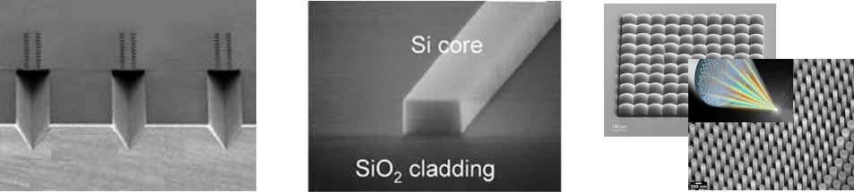
Silicon Photonics and the AI Interconnect Bottleneck
Perhaps the most cutting-edge sector of the specialty surge is silicon photonics and co-packaged optics (CPO). As AI models grow in size, the bottleneck for performance is no longer just the compute power of the chip, but the speed at which data can move between chips. Traditional copper wiring is reaching its physical limits in terms of bandwidth and power consumption.
Silicon photonics addresses this by using light (photons) instead of electricity (electrons) to transmit data. This technology replaces metal traces with optical waveguides. In CPO configurations, the optical components are integrated directly onto the same package as the processor. This requires the assembly of diverse components: lasers, waveguides, microlenses, and opto-electronic converters.
The manufacturing challenges here are multi-faceted. V-grooves must be etched into the silicon to hold optical fibers with sub-micron accuracy. Waveguides must be formed with incredibly smooth surfaces to prevent light scattering. Any misalignment in the multi-die assembly process can result in significant signal loss. As data centers transition to 800G and 1.6T speeds, the success of silicon photonics will depend on the industry’s ability to perform high-throughput inspection of these complex, multi-material modules.
Industry Analysis: The Economic and Technical Implications
The common thread across MEMS, CIS, power devices, and photonics is the necessity of "process control." In the traditional logic world, the goal is "shrinkage"—making features smaller. In the specialty world, the goal is "precision and diversification"—making features more reliable, more uniform, and more cost-effective across a variety of materials.
Industry analysts suggest that the "Cost of Ownership" (CoO) is the most critical metric for manufacturers in this segment. While a leading-edge logic fab might spend billions on Extreme Ultraviolet (EUV) lithography, specialty fabs require metrology and inspection tools that can handle non-standard wafer thicknesses and transparent substrates (like SiC) without ballooning the cost of the final product.
Furthermore, the surge in specialty devices is driving a secondary market for refurbished and specialized semiconductor manufacturing equipment. Companies like Onto Innovation, KLA, and Applied Materials are increasingly developing tools specifically designed for the "More than Moore" market, focusing on 3D metrology and all-surface inspection.
Conclusion and Future Outlook
The specialty device surge is not a temporary trend but a fundamental realignment of the semiconductor industry. As the world becomes more connected and more reliant on automated systems, the demand for sensors, high-efficiency power converters, and optical data links will only intensify.
The successful manufacturers of the next decade will be those who can master the "Specialty Surge" by implementing advanced metrology and intelligent inspection systems. By tightening the feedback loops in the manufacturing process, these companies can stay within increasingly narrow process windows, ensuring that the "unsung heroes" of modern life continue to perform their critical functions at high volume and low cost. The transition to larger wafers and more complex architectures is well underway, and while the challenges are significant, the potential for innovation remains boundless. In the coming years, the ability to measure what matters—shape, thickness, and material integrity—will be the defining factor in the global semiconductor race.