
The global semiconductor landscape is currently undergoing a seismic shift as artificial intelligence (AI) migrates from centralized data centers to the network edge, necessitating a new generation of hardware that balances high-speed performance with extreme energy efficiency. At the center of this transition is LPDDR5 (Low Power Double Data Rate 5) memory, a technology that has rapidly evolved from a niche mobile component into the primary memory architecture for a vast array of sophisticated applications. While large-scale training of generative AI models continues to rely on high-bandwidth memory (HBM) and standard DDR5 in massive server farms, the practical implementation of AI in the real world—often referred to as edge inferencing—requires a different set of engineering priorities. Devices such as autonomous vehicles, high-end smartphones, industrial IoT sensors, and portable medical equipment operate under strict thermal envelopes and battery constraints, making the efficiency-to-performance ratio of LPDDR5 indispensable.
The Shift Toward Edge Inferencing
Inferencing at the edge represents a departure from the traditional cloud-computing model where data is sent to a remote server, processed, and returned. As Steve Woo, a fellow and distinguished inventor at Rambus, notes, edge devices have fundamentally different requirements than the high-performance computing (HPC) clusters used for training Large Language Models (LLMs). Training requires massive throughput and the ability to handle vast datasets across thousands of GPUs. In contrast, edge inferencing is often characterized by the need for real-time responsiveness, privacy, and low latency, all while operating on a limited power budget.
The physical constraints of edge hardware are a primary driver for the adoption of LPDDR5. Most edge devices are price-sensitive and must adhere to small form factors, limiting the physical area available for memory modules. Furthermore, because many of these devices run on batteries, every milliwatt saved in memory operations translates directly into longer device longevity or the ability to allocate more power to the processor for complex computations. LPDDR5 addresses these challenges by offering a significant leap in data transfer rates without the proportional increase in power consumption that typically accompanies such gains.
A Chronological Evolution of Low-Power Memory
To understand the dominance of LPDDR5, it is essential to trace the chronology of the Low Power Double Data Rate standard, which is overseen by JEDEC (Joint Electron Device Engineering Council). The journey began with the original LPDDR1, which was essentially a lower-voltage version of standard DDR. However, as the smartphone revolution took hold in the late 2000s, the divergence between mobile and desktop memory became more pronounced.
LPDDR4, introduced around 2014, was a landmark standard that utilized a dual-channel architecture to improve efficiency. It provided a data rate of 3200 MT/s (MegaTransfers per second), which was later boosted to 4266 MT/s with LPDDR4X. LPDDR4X was a critical interim step, reducing the I/O voltage (Vdq) from 1.1V to 0.6V, significantly lowering power consumption during data transfers.
The JEDEC committee officially published the LPDDR5 standard (JESD209-5) in February 2019. This version was designed specifically to handle the demands of 5G connectivity and early-stage mobile AI. By 2021, the industry saw the introduction of LPDDR5X, which pushed the boundaries even further, reaching speeds of up to 8.5 Gbps. The timeline of adoption shows a clear trajectory: while LPDDR4 served the industry for nearly a decade, the transition to LPDDR5 has been accelerated by the sudden explosion of AI-integrated consumer electronics and the automotive industry’s move toward software-defined vehicles.

Technical Superiority and Comparative Data
The technical advantages of LPDDR5 over its predecessor, LPDDR4, are substantial and measurable. One of the most significant changes is the increase in data rates. While LPDDR4 peaked at 4266 MT/s, LPDDR5 started at 5500 MT/s and quickly scaled to 6400 MT/s. This represents a nearly 50% increase in bandwidth, which is vital for feeding the hungry neural processing units (NPUs) found in modern SoCs (System on Chips).
Beyond raw speed, LPDDR5 introduces several architectural innovations aimed at power conservation:
- Dynamic Voltage and Frequency Scaling (DVFS): LPDDR5 allows the system to adjust both the frequency and the voltage based on the workload. For low-intensity tasks, the memory can drop to a lower power state more effectively than previous generations.
- Deep Sleep Mode: This feature reduces power consumption by up to 40% during idle periods compared to LPDDR4, a critical factor for "always-on" devices like smart home assistants.
- Bank Grouping: Similar to standard DDR4/5, LPDDR5 utilizes a bank grouping architecture. This allows for more efficient data access patterns, reducing the latency involved in switching between different memory banks.
- WCK (Write Clock): LPDDR5 moved to a new clocking architecture using a Write Clock (WCK) that is twice the frequency of the command/address clock. This allows for high-speed data transfers without requiring the entire memory interface to run at peak frequency, saving energy.
According to industry data, LPDDR5 provides an approximately 20% reduction in power consumption compared to LPDDR4X while delivering significantly higher throughput. In the context of a smartphone or an IoT gateway, this 20% saving can be the difference between a device that lasts a full day and one that requires mid-day charging.
Packaging and Capacity Innovations
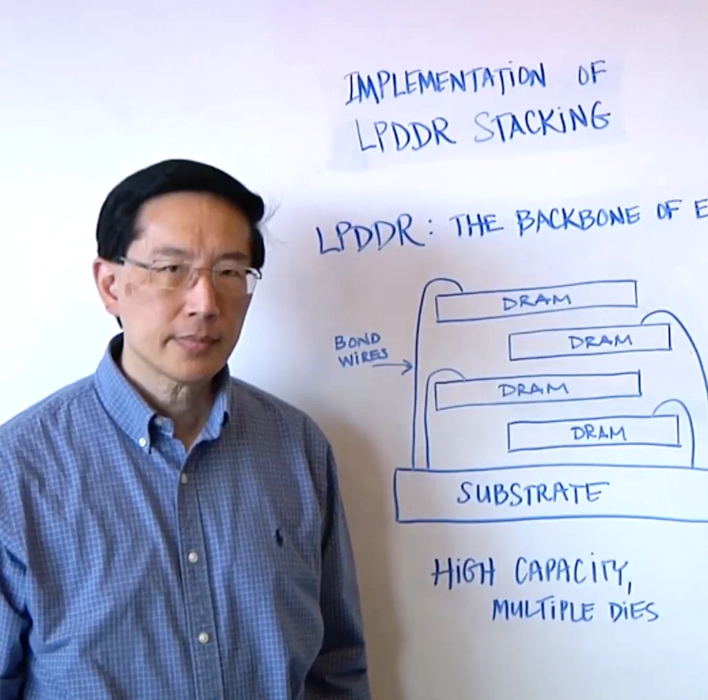
A major challenge at the edge is the physical limitation of memory capacity. Because edge devices cannot house the massive DIMM slots found in servers, they rely on specialized packaging techniques. Steve Woo highlights that LPDDR5 can be packaged in several ways to maximize density without increasing the footprint.
One of the most common methods is Package-on-Package (PoP), where the LPDDR5 die is stacked directly on top of the application processor. This not only saves board space but also shortens the signal paths, which reduces power loss and improves signal integrity at high frequencies. For automotive and industrial applications where vibration and thermal cycling are concerns, discrete LPDDR5 chips are often soldered directly to the PCB (Printed Circuit Board) using Ball Grid Array (BGA) packaging.
To address the growing memory requirements of edge AI—which can require several gigabytes of RAM just to hold the model weights—manufacturers are now producing multi-die packages (MDP). By stacking multiple LPDDR5 dies within a single package, vendors can offer 16GB, 24GB, or even 32GB of low-power memory in a footprint no larger than a postage stamp.
Industry Perspectives and Market Adoption
The adoption of LPDDR5 is not limited to the mobile sector; it is seeing rapid uptake in the automotive and industrial sectors. Representatives from major semiconductor firms, including Rambus, Micron, and Samsung, have noted that the "intelligence" of a device is now directly tied to its memory bandwidth.

In the automotive sector, Advanced Driver Assistance Systems (ADAS) and autonomous driving levels 2 and 3 require massive amounts of real-time data processing from cameras, LiDAR, and radar sensors. The industry has reacted by shifting away from standard DDR and toward LPDDR5 because the latter can handle the high-temperature environments of a vehicle engine bay or cabin while maintaining the high data rates needed for safety-critical decision-making.
Industry analysts suggest that the "total cost of ownership" for edge devices is being redefined. While LPDDR5 carries a slight price premium over LPDDR4, the savings in thermal management hardware (such as smaller heat sinks) and the improved user experience (faster app loading and better AI features) justify the investment.
Broader Impact and Future Implications
The rise of LPDDR5 is more than just a technical upgrade; it is an enabler of the next generation of computing. By providing the bandwidth necessary for local inferencing, LPDDR5 is facilitating a more private and secure AI ecosystem. When a device can process voice commands or facial recognition locally using LPDDR5-backed NPUs, sensitive data does not need to be transmitted to the cloud, reducing the risk of data breaches and lowering the bandwidth costs for consumers.
Looking ahead, the roadmap for low-power memory continues to evolve. While LPDDR5 is the current "sweet spot" for many applications, the industry is already looking toward LPDDR6. The next standard is expected to focus even more heavily on "Memory-Centric Computing," where more processing happens near or within the memory itself to minimize the energy-intensive movement of data across the bus.
In conclusion, LPDDR5 has become the memory of choice because it solves the fundamental paradox of edge computing: the need for high-performance capabilities within a low-power, space-constrained environment. As Steve Woo and other experts have pointed out, the ability to pack more capacity and speed into smaller, more efficient packages is the key to unlocking the full potential of AI at the edge. Whether it is in a smartphone, a self-driving car, or an industrial robot, LPDDR5 is the silent engine driving the modern digital experience, proving that in the world of semiconductors, efficiency is just as valuable as speed.