
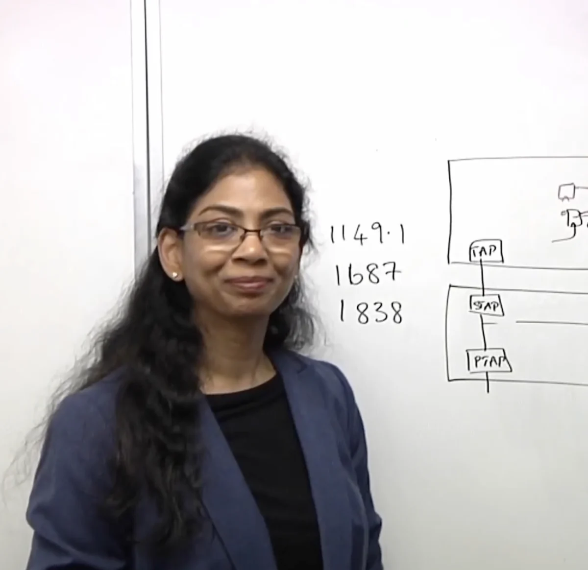

As semiconductor manufacturing descends into the angstrom era, the physical complexity of integrated circuits (ICs) has surged, creating a bottleneck in post-fabrication testing. Modern chip architectures—characterized by multi-die configurations, 2.5D/3D packaging, and advanced FinFET and gate-all-around (GAA) transistor structures—generate an unprecedented volume of diagnostic data. This data deluge, if not managed with sophisticated Design-for-Test (DFT) methodologies, threatens to extend time-to-market and inflate production costs. To address these challenges, industry experts, including Vidya Neerkundar, director of DFT product management at Siemens EDA’s Tessent Division, are advocating for a fundamental shift in how testing standards and data bandwidth are managed throughout the chip lifecycle.
The Data Explosion: Why Testing Complexity is Escalating
The transition from legacy planar transistors to 3D structures like FinFETs and upcoming nanosheet designs has introduced new failure modes. At 7nm, 5nm, and 3nm process nodes, the sensitivity to manufacturing defects is significantly higher than at 28nm or 45nm nodes. A single defect in a microscopic feature can lead to systematic reliability failures, requiring more comprehensive test patterns to ensure functional integrity.
Historically, testing involved simple scan chains that checked for "stuck-at" faults. Today, however, the industry must account for transition delays, bridging faults, and complex signal integrity issues that only manifest under high-frequency operation. According to industry data, the amount of test data required for a single chip has increased by roughly 20% to 30% per year over the last decade. This creates a "bandwidth wall": the internal test access ports (TAP) and the physical pins available on the chip package cannot move the required volume of data fast enough to keep test times economically viable.
Chronology of DFT Evolution
The evolution of testing methodology has tracked closely with the advancement of lithography and packaging techniques.

- 1990s – Early 2000s: Industry reliance on JTAG (IEEE 1149.1) and simple scan-based testing. This era focused primarily on structural connectivity and basic logic verification.
- 2005 – 2015: The introduction of scan compression technologies allowed engineers to shrink test patterns, enabling higher fault coverage without requiring exponentially more pins.
- 2015 – 2020: The rise of FinFETs necessitated the implementation of high-speed at-speed testing (AST) to detect subtle timing-related defects that were previously ignored.
- 2020 – Present: The move toward chiplets and 3D-IC architectures. The focus has shifted toward "Known Good Die" (KGD) testing, where each component must be verified before integration into a complex system-in-package (SiP).
Managing the Data Bandwidth Bottleneck
One of the primary strategies discussed by industry leaders involves the intelligent compression and streaming of test data. Siemens EDA’s Tessent division, among others, has focused on creating "test highways"—on-chip networks that treat test data similar to how high-speed packet-switched data is routed in a standard SoC.
By decoupling the test pattern delivery from the external tester, companies can utilize high-bandwidth internal interfaces to move data to the specific blocks being tested. This "streaming" approach minimizes the time a device spends on the Automated Test Equipment (ATE), which is often the most expensive component of the semiconductor manufacturing process. Reducing test time by even a few seconds per chip translates into millions of dollars in savings for high-volume consumer electronic products.
The Role of Standards in Modern DFT
Standardization efforts have been critical in navigating the shift toward chiplet-based designs. The IEEE 1838 standard, specifically designed for 3D-IC testing, provides a framework for testing individual dies within a stack. Before the formalization of these standards, companies were forced to develop proprietary, non-interoperable test protocols, which complicated the integration of IP from multiple vendors.
Neerkundar and other industry stakeholders emphasize that IEEE 1838 is not merely a recommendation but a necessity for modern heterogeneous integration. It allows the test data to move through the "vertical" interfaces of a 3D-IC, ensuring that a logic die can verify the status of a memory die without needing direct physical access to the memory’s pins.
Supporting Data: The Economic Impact of Reliability
The economic implications of inadequate testing are profound. According to recent semiconductor industry reports, the "cost of quality" (which includes scrap, rework, and return merchandise authorizations) can account for up to 10% of total manufacturing costs for advanced nodes.

- Test Time Reduction: By adopting hierarchical DFT, manufacturers have reported a 40% reduction in overall test time compared to flat, monolithic test structures.
- Fault Coverage: Advanced at-speed testing is now reaching upwards of 99% of total transition faults, a critical benchmark for automotive and mission-critical AI hardware where zero-failure rates are the industry standard.
- ATE Utilization: As the cost of high-end ATE machines approaches $5 million to $10 million per unit, maximizing throughput—the number of chips tested per hour—has become the primary driver of profitability in the backend assembly and test (OSAT) sector.
Broader Implications and Future Outlook
The shift toward more robust, data-intensive testing is occurring at the same time the industry is facing a shortage of specialized talent. As designs become more complex, the gap between traditional design engineers and DFT specialists is closing. Modern EDA tools are now automating much of the test pattern generation, allowing designers to focus on architectural reliability rather than manual scan-chain insertion.
However, the future poses even greater challenges. With the industry moving toward 2nm and beyond, thermal management during the test process has become a major concern. Running a full suite of at-speed tests can cause a chip to overheat, leading to false negatives or even physical damage to the wafer. "Thermal-aware testing," where test patterns are distributed across the chip to avoid localized hotspots, is currently the subject of intense R&D within the EDA community.
Furthermore, as Artificial Intelligence is increasingly integrated into semiconductor design, AI-driven test pattern generation is expected to become the next frontier. By using machine learning models to predict where defects are most likely to occur based on historical fabrication data, manufacturers can create "smarter" test sets that target high-risk areas, further reducing the total volume of data required to achieve the same level of confidence.
Conclusion: Balancing Efficiency and Reliability
The challenge of testing in the current semiconductor landscape is a balance between extreme technical precision and rigid economic constraints. As Vidya Neerkundar and her peers suggest, the solution does not lie in a single "silver bullet" technology but in a holistic approach that combines advanced EDA software, standardized interfaces, and intelligent data management.
For the semiconductor industry, the objective remains clear: as the physical limits of Moore’s Law are tested, the reliability of the resulting hardware must not follow suit. Through the continued adoption of hierarchical DFT, streaming test architectures, and industry-wide standardization, the sector is well-positioned to maintain the rigorous quality standards required by the next generation of computing, from mobile devices and AI data centers to automotive autonomous driving systems. The transition is complex, but the path toward more efficient, data-driven, and reliable chip production is already being paved by these technological advancements.
