
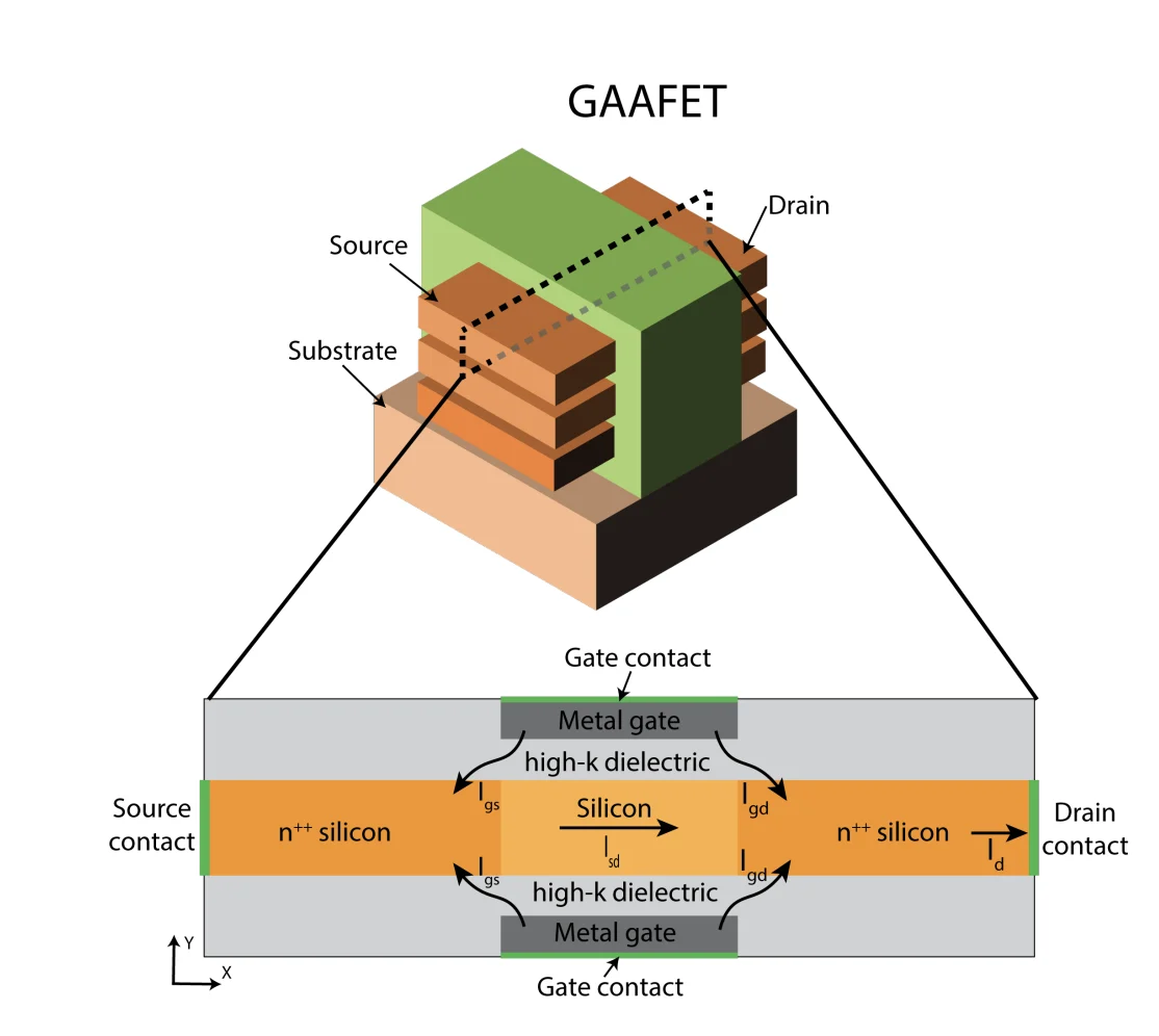

The semiconductor industry is currently navigating a critical transition as it moves beyond the limitations of Fin Field-Effect Transistors (FinFETs) toward Gate-All-Around Field-Effect Transistors (GAAFETs). As chip manufacturers push toward increasingly dense nodes, maintaining electrostatic control over the transistor channel has become the defining challenge of modern lithography and architecture design. A recent study conducted by researchers at Sandia National Laboratories and the Luxembourg Institute of Science and Technology has shed new light on a persistent performance hurdle: unexpected leakage paths that threaten the efficiency of next-generation GAAFET architectures.
The Evolution of Transistor Architecture
For over a decade, FinFETs have served as the workhorse of the semiconductor industry. By utilizing a three-dimensional "fin" structure, FinFETs allowed engineers to increase drive current while maintaining a smaller footprint than traditional planar transistors. However, as scaling continues toward the sub-3nm regime, the physical limitations of the fin structure—specifically the inability to fully wrap the gate around the channel—have resulted in increased short-channel effects and parasitic leakage.
GAAFETs were introduced as the logical successor, offering a nanosheet or nanowire configuration where the gate material completely surrounds the channel. This "all-around" control theoretically eliminates sub-threshold leakage by maximizing the electrostatic influence of the gate. Yet, as the industry begins to scale these devices in commercial production, empirical measurements have revealed anomalous behavior: a significant rise in drain current at negative gate voltages, a phenomenon that contradicts classical thermionic emission models.
Identifying the Leakage Anomaly
The research paper, published in October 2026, investigates why GAAFETs exhibit this non-ideal current increase when the gate is biased negatively. The team, led by Denis Mamaluy and his colleagues, posits that the leakage is not merely a byproduct of fabrication defects but a fundamental interaction involving the high-k dielectric layer used to insulate the gate.
According to the study, this leakage is driven by direct gate-to-drain tunneling, which is further exacerbated by a phenomenon termed Drain-Induced Dielectric Barrier Lowering (DIDBL). In conventional transistor theory, the barrier at the drain-gate interface is expected to remain robust. However, the simulation data suggests that at advanced nodes, the proximity of the drain contact to the gate dielectric effectively lowers the energy barrier for electrons, creating a "leaky" path that bypasses the intended switching mechanism of the transistor.

Methodology: Predictive First-Principles Simulations
To map these microscopic pathways, the research team utilized charge-self-consistent Non-Equilibrium Green Function (NEGF) simulations. This computational approach, specifically leveraging the Contact Block Reduction (CBR) method, allows for the atomistic modeling of electron transport.
Unlike traditional drift-diffusion models, which often rely on macroscopic approximations that fail at the nanometer scale, the NEGF-CBR framework accounts for the quantum mechanical nature of electron tunneling. By spatially resolving the leakage current, the researchers were able to visualize exactly where the dielectric barrier fails. This level of granularity provides a digital "roadmap" for engineers to potentially re-engineer the dielectric stack or modify the spacing between the drain and the gate to suppress the tunneling effect.
Chronology of GAAFET Scaling Challenges
The industry’s path to GAAFET adoption has been marked by a series of technical milestones and obstacles:
- 2018–2020: Major foundries begin pilot production of nanosheet-based test structures, moving away from FinFET prototypes.
- 2022: The first high-volume manufacturing nodes using GAA architectures are announced, emphasizing the need for improved power-performance-area (PPA) metrics.
- 2024: Early performance reports from advanced nodes indicate higher-than-expected standby power consumption, leading to industry-wide investigations into leakage mechanisms.
- October 2026: The publication of the Sandia-Luxembourg study provides the first comprehensive, atomistic explanation for the specific "DIDBL" leakage pathway, offering a potential path forward for design optimization.
Supporting Data and Physical Implications
The simulations performed by the team reveal a non-linear relationship between gate voltage and drain current that traditional models consistently underestimate. In a standard FinFET, the "off-state" current is largely controlled by the height of the potential barrier. In the GAAFETs analyzed, the direct tunneling component becomes dominant at low voltages, effectively creating a "floor" for power consumption that cannot be lowered by simply adjusting the gate voltage.
The research highlights that as the dielectric thickness is scaled down to support higher gate capacitance, the tunneling probability increases exponentially. If left unaddressed, this leakage could negate the power-efficiency gains expected from the transition to GAAFETs, particularly for battery-constrained applications such as mobile computing and artificial intelligence accelerators, which rely on low-power standby modes.
Industry and Academic Reactions
While the findings have yet to be fully integrated into commercial foundry processes, the academic community has responded with cautious optimism. Experts in the field of device physics suggest that this research provides a necessary framework for "designing out" the leakage.

"The identification of DIDBL as a primary culprit for non-thermionic leakage is a significant step toward stabilizing the next generation of transistors," noted a senior device engineer familiar with the study. "By understanding the spatial resolution of these paths, we can move from reactive troubleshooting—where we guess why a chip is leaking—to proactive design, where we tailor the geometry of the gate-drain interface to physically block these pathways."
Broader Impact on Semiconductor Scaling
The implications of the Sandia and Luxembourg Institute findings extend beyond current production cycles. As the semiconductor roadmap pushes toward even smaller dimensions, such as 1nm and beyond, the precision required for material placement and interface engineering will only increase.
If foundries can utilize these first-principles simulations to refine their chemical vapor deposition (CVD) or atomic layer deposition (ALD) processes, they may be able to extend the lifespan of GAAFET technology for several additional years. The ability to model these tunneling paths in a predictive manner reduces the cost of "trial-and-error" fabrication, which has become prohibitively expensive due to the complexity of Extreme Ultraviolet (EUV) lithography and multi-patterning techniques.
Conclusion and Future Outlook
The research titled "Revealing New Leakage Paths in GAAFETs using Predictive First-Principles Simulations" serves as a vital bridge between theoretical quantum mechanics and practical semiconductor manufacturing. By identifying the specific mechanisms behind gate-drain leakage, the authors have provided a roadmap for the next phase of transistor evolution.
As the industry continues to scale, the focus will likely shift from simply increasing transistor density to optimizing the microscopic interfaces that govern electron transport. The collaboration between Sandia National Laboratories and the Luxembourg Institute of Science and Technology demonstrates the importance of interdisciplinary research in overcoming the physical limits of Moore’s Law. Whether through the introduction of new dielectric materials or refined geometric spacing, the industry now has the data required to address the "leakage floor" and ensure that GAAFETs deliver on their promise of superior performance and efficiency for the next decade of technological advancement.
For engineers and designers, the message is clear: the path to the future is not just about making things smaller, but about understanding the fundamental quantum interactions that occur at the heart of the silicon. As this research moves from the laboratory to the fab, it will undoubtedly influence the architecture of the next generation of high-performance computing devices.
