
The semiconductor industry is currently undergoing a fundamental transformation as Artificial Intelligence (AI) transitions from a supplementary tool to a core driver of Electronic Design Automation (EDA). While AI has been embedded in EDA algorithms for decades to assist with optimization and heuristic-based problem solving, the emergence of generative and agentic AI marks a new era in chip design. This evolution is categorized by industry leaders, such as Ziyad Hanna, corporate vice president at Cadence, into a multi-tiered framework of autonomy that mirrors the developmental stages of self-driving vehicles. As chip complexity reaches unprecedented levels—with designs now exceeding billions of transistors—the integration of smarter, more autonomous systems is no longer an optional luxury but a technical necessity for maintaining the pace of Moore’s Law.
The Evolution of Intelligent Silicon Design
The history of EDA is defined by the constant struggle to manage complexity. In the 1980s and 1990s, EDA focused on automating manual tasks such as schematic capture and basic routing. By the early 2010s, Machine Learning (ML) began to appear in specialized applications, primarily for predictive modeling of Power, Performance, and Area (PPA). These early implementations were "closed-loop" systems where the AI operated within narrow parameters to refine existing designs.
Today, the focus has shifted toward "Agentic AI." Unlike traditional AI, which follows a predefined set of instructions, agentic AI is capable of proactive decision-making. These agents can perceive their environment, reason through complex design constraints, and take actions to achieve a specific goal, such as reducing the footprint of a logic block or optimizing the power delivery network of a 3nm processor. This shift represents the transition from AI as a feature to AI as an autonomous collaborator.
Defining the Five Levels of EDA Autonomy
To provide a roadmap for this technological shift, the industry has adopted a classification system for autonomy in chip design. This framework, popularized by Cadence and other major EDA vendors, establishes five distinct levels of progression:
- Level 1: Assistance and Visualization. At this level, AI provides insights and data visualization to help human engineers make better decisions. It might highlight potential congestion areas in a layout or suggest minor adjustments to timing constraints.
- Level 2: Partial Automation. The AI takes over specific, well-defined tasks under human supervision. For example, an AI tool might automatically route a specific subsystem, but the engineer must still review and approve the final path.
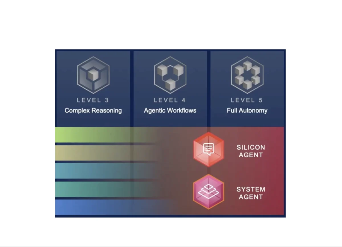
- Level 3: Conditional Autonomy. The system can manage a significant portion of the design flow independently. It can make tactical decisions and optimize sub-blocks, but it requires a human to intervene when it encounters "edge cases" or conflicting constraints that it cannot resolve.
- Level 4: High Autonomy. At this stage, the AI can complete complex, high-level tasks across various stages of the design flow—such as synthesis and physical implementation—with minimal human intervention. It can self-correct based on simulation results and iterate through thousands of permutations to find the optimal design point.
- Level 5: Full Autonomy. This represents the "lights-out" design environment. A high-level specification is provided by a human, and the AI handles the entire process from RTL (Register Transfer Level) to GDSII (the final layout format for manufacturing), including verification and sign-off, without human oversight.
Currently, the industry is largely operating between Level 2 and Level 3, with aggressive research and development pushing toward Level 4 for specific localized tasks.
The Rise of Agentic and Generative AI
The introduction of Large Language Models (LLMs) and generative AI has provided a new interface for EDA. Engineers are now using generative models to assist in writing Hardware Description Language (HDL) code, such as Verilog or VHDL. However, the true breakthrough lies in the "agentic" nature of these models.

Agentic AI systems do not merely generate code; they can execute it, observe the errors, and rewrite the code until it passes verification. This creates a self-healing design loop. For instance, in verification—which currently accounts for nearly 70% of the total design cycle—AI agents can automatically generate test benches and coverage reports, identifying bugs that might have been missed by human-authored tests. This proactive capability is essential as the industry moves toward 2nm and 1.4nm process nodes, where the physical phenomena affecting chip performance become increasingly non-linear and difficult to model manually.
Supporting Data and Market Dynamics
The economic imperative for AI in EDA is supported by significant market growth and resource constraints. According to recent industry reports, the global EDA market was valued at approximately $15.2 billion in 2023 and is projected to reach over $22 billion by 2028, growing at a CAGR of 10.5%. This growth is driven by the demand for specialized chips for AI data centers, automotive electronics, and 5G/6G infrastructure.
Furthermore, the semiconductor industry faces a chronic talent shortage. Estimates from the Semiconductor Industry Association (SIA) suggest that by 2030, the U.S. alone could face a deficit of 67,000 technicians, computer scientists, and engineers. AI serves as a "force multiplier," allowing a single engineer to manage more complex designs and reducing the time-to-market (TTM) for new products. Preliminary data from pilot programs at major chipmakers indicate that AI-driven placement and routing can reduce design time by up to 30% while improving power efficiency by 10% to 15%.
Technical Challenges: Traceability and Explainability
Despite the rapid advancement, significant hurdles remain. Two of the most critical challenges are traceability and explainability. In the semiconductor world, where a single mask set for a leading-edge node can cost upwards of $10 million, "black box" solutions are unacceptable.
Traceability refers to the ability to track every design decision back to its source. If an AI agent modifies a timing path, engineers need to know which data or constraint triggered that change. This is essential for debugging and for meeting safety standards in industries like aerospace and automotive.
Explainability involves understanding the "why" behind an AI’s decision. Because deep learning models operate on high-dimensional data, their logic can be opaque. If an AI tool suggests a radical new floorplan that differs from traditional engineering intuition, the human designer must be able to verify that the suggestion is based on sound physical principles rather than a "hallucination" or a statistical fluke. Developing "Explainable AI" (XAI) for EDA is a major focus for companies like Cadence, Synopsys, and Siemens EDA.
Industry Reactions and Official Responses
Leaders across the semiconductor ecosystem have expressed a cautious but optimistic view of this transition. Ziyad Hanna of Cadence has emphasized that while AI will handle the "heavy lifting" of optimization, the role of the human engineer will shift toward high-level architecture and system-level intent.

In a similar vein, executives at Synopsys have noted that their AI-driven design suites (such as DSO.ai) are already being used in production environments for high-performance computing (HPC) chips. The general consensus among EDA vendors is that AI is not a replacement for human ingenuity but a sophisticated toolset that enables engineers to explore a much wider design space than previously possible.
Hardware engineers, however, have raised concerns regarding data privacy and IP protection. Because many generative AI models are trained on vast datasets, there is a risk of proprietary design patterns being inadvertently shared or leaked if the models are not deployed within secure, private environments.
Broader Impact and Implications
The long-term implications of AI-driven EDA extend beyond the engineering lab. By reducing the cost and time required to design high-performance chips, AI could democratize silicon innovation. Smaller startups, which were previously priced out of the custom silicon market due to the high cost of EDA licenses and engineering hours, may find it easier to develop application-specific integrated circuits (ASICs).
Moreover, as AI becomes more integrated into the design flow, we can expect a shift in the global supply chain. The ability to rapidly iterate on chip designs will allow for more "localized" or "bespoke" silicon tailored to specific software workloads, potentially reducing the reliance on general-purpose processors.
In conclusion, the step-by-step application of AI in EDA is moving from a sequence of isolated optimizations toward a holistic, autonomous design ecosystem. As the industry advances through the levels of autonomy, the focus will remain on balancing the raw speed and optimization power of AI with the necessary guardrails of traceability, explainability, and security. The roadmap to Level 5 autonomy is being paved today, one agentic algorithm at a time, ensuring that the next generation of silicon is not just smaller and faster, but designed with a level of intelligence that matches the tasks it is destined to perform.
