
The semiconductor industry is currently navigating a period of unprecedented complexity as innovation in chip development and manufacturing continues to accelerate without signs of stabilization. The transition toward ever-larger chips characterized by smaller geometries—approaching the 3-nanometer and 2-nanometer thresholds—has introduced a suite of physical and systemic challenges that traditional methodologies are struggling to address. Simultaneously, intense competitive pressures are drastically compressing Time to Market (TTM), placing immense strain on engineering and project teams to deliver high-performance silicon that meets stringent safety and reliability standards. This environment has necessitated a fundamental shift in how chips are tested and monitored, leading to a significant convergence of Design for Test (DFT) techniques and Silicon Lifecycle Management (SLM).
This evolution was a central theme at the recent IEEE International Reliability Physics Symposium (IRPS), where Adam Cron, a Distinguished Architect at Synopsys, detailed the integration of in-system testing and SLM data. The core of the discussion focused on how the reliability community can leverage these innovations to manage the entire lifespan of a chip, from its initial laboratory bring-up and high-volume production to its active mission life in the field.
The Evolution of Semiconductor Testing Methodologies
The history of semiconductor testing has transitioned from simple functional checks to a highly sophisticated ecosystem of automated and embedded solutions. Historically, chip testing was primarily a gatekeeping function performed at the end of the manufacturing process. Automated Test Equipment (ATE) was used to test chips at the wafer and package levels, ensuring that only functional units were shipped to customers.
In the current landscape, the emergence of 3D chip designs and heterogeneous integration—where multiple dies are stacked or placed in a single package—has added layers of complexity. Testing must now occur not only at the individual die level but also at the stack level to ensure interconnect integrity. This requires a robust set of patterns generated by Automatic Test Pattern Generation (ATPG) tools. These tools utilize sophisticated fault models, such as stuck-at, path delay, and IDDQ (Quiescent Current), to represent potential silicon defects. By implementing scan chains—where flip-flops are connected into serial chains—engineers can load specific values and scan out results, making the detection of manufacturing defects practical at scale.

As chips moved into safety-critical sectors like automotive (ISO 26262 standards) and aerospace, the industry adopted Built-In Self-Test (BIST) for both logic (LBIST) and memory (MBIST). These techniques allow the chip to generate its own internal test patterns and verify the results autonomously. This capability marked the beginning of the shift from external manufacturing tests to in-field diagnostic capabilities.
The Paradigm Shift Toward Silicon Lifecycle Management
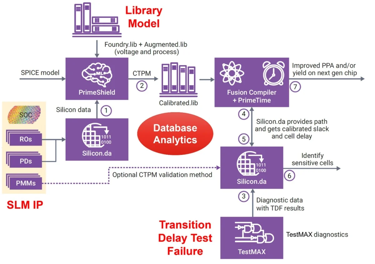
While traditional DFT focuses on identifying defects during or immediately after manufacturing, Silicon Lifecycle Management (SLM) represents a broader, more holistic approach. SLM tracks the health, performance, and reliability of a device from the design phase through its entire operational life. This proactive stance is becoming critical as advanced nodes become more susceptible to aging effects, such as Bias Temperature Instability (BTI) and Electromigration (EM).
The integration of in-silicon monitors and sensors is the technical foundation of SLM. These embedded IP blocks, such as ring oscillators, provide real-time data on silicon performance. For instance, a ring oscillator consisting of an odd number of inverting gates creates a series of clock pulses that can be counted over a specific interval. If the pulse count decreases over time under identical operating conditions, it serves as a measurable indicator of silicon degradation due to aging. This data allows system operators to perform preventive maintenance, replacing components before a catastrophic failure occurs—a requirement that is non-negotiable in autonomous driving and medical applications.
Strategic Chronology of the Silicon Lifecycle
The implementation of SLM follows a structured chronology that begins long before a chip reaches a consumer:
- Design and Integration Phase: Engineers embed SLM IP, including thermal sensors, process monitors, and voltage monitors, into the SoC (System on Chip) architecture.
- Manufacturing and Wafer Test: During production, these monitors provide data on process variations across the wafer, helping to bin parts more accurately and improve initial yield.
- System Bring-up: In the lab, SLM data helps debug complex timing issues and validates that the silicon matches the simulated models.
- In-Field Mission Mode: Once deployed, the chip continues to monitor its own environment and health. It can detect "soft errors" caused by alpha particles or cosmic rays using Error Correcting Code (ECC) and parity bits.
- Data Feedback Loop: Data from failed or degrading parts in the field is fed back to the design teams. This information is used to refine technology libraries and improve the design of next-generation chips.
Data-Driven Optimization: Vmin Prediction and Library Characterization
One of the most impactful applications of the DFT and SLM convergence is the optimization of the minimum operating voltage (Vmin). Historically, chip designers have applied generous "guard bands"—extra voltage margins—to ensure that a chip remains functional as it ages and its performance slows down. However, these guard bands lead to overdesign, resulting in higher power consumption and heat generation.

By utilizing accurate field data from SLM IP, often processed through AI and machine learning algorithms, manufacturers can predict Vmin with much higher precision. This allows chips to operate closer to their theoretical limits, reducing power consumption in data centers and extending battery life in mobile devices.
Furthermore, SLM is revolutionizing library characterization. Semiconductor design relies on libraries that model how transistors and gates will behave under various conditions. By comparing actual silicon data—such as threshold voltage (Vth) deviations—with predicted model values, engineers can refine their libraries. This ensures that the "digital twin" of the chip used during the design phase is an accurate reflection of the physical silicon produced in the fab.
Resilience Through Self-Repair and Redundancy
The industry is also seeing a rise in "self-healing" silicon. As interconnect standards like UCIe (Universal Chiplet Interconnect Express), AIB (Advanced Interface Bus), and HBM4 (High Bandwidth Memory 4) become standard, they are increasingly incorporating spare lanes and pins. If an SLM monitor detects an impending failure in a specific signal path, the system can automatically "swap" the failing lane for a spare one without interrupting service.
For logic, techniques such as Dual Modular Redundancy (DMR) and Triple Modular Redundancy (TMR) are employed. In a TMR setup, three registers perform the same operation, and a "voter" circuit determines the output based on the majority. If one register fails or experiences a bit-flip, it is effectively outvoted by the functional registers, ensuring system uptime. In memories, which can account for over 50% of a chip’s area, Built-In Self-Repair (BISR) and column/row redundancy are used to bypass defective memory cells identified during BIST routines.
Industry Implications and Future Outlook
The transition toward a data-centric approach to silicon reliability has significant implications for the global supply chain. For hyperscalers and automotive OEMs, the ability to monitor "fleets" of chips rather than individual units provides a macro-level view of hardware health. This "fleet analytics" approach enables cloud providers to predict which server blades are likely to fail, allowing for seamless workload migration and reducing downtime.

Industry experts suggest that the demand for SLM solutions will continue to grow as the industry moves toward 2nm processes and complex 2.5D/3D packaging. The sheer density of transistors and the proximity of heat-generating components in these designs make real-time monitoring a necessity rather than a luxury.
As Adam Cron noted in his conclusion at the IRPS, the combination of SLM and traditional DFT provides a rich trove of data that is only beginning to be fully exploited. With the integration of AI-driven analytics, the next generation of semiconductors will not only be faster and smaller but also significantly more intelligent regarding their own health and longevity. The goal of "zero-ppm" (zero defects per million) in safety-critical applications is becoming more attainable as the industry moves away from reactive testing toward a model of continuous, lifelong silicon oversight.
