
The semiconductor industry is currently navigating a pivotal transition as traditional two-dimensional (2D) System-on-Chip (SoC) designs encounter the physical and economic limits of Moore’s Law. Driven by the relentless demands of generative artificial intelligence (AI), high-performance computing (HPC), and massive data-centric workloads, manufacturers are increasingly turning to 2.5D and 3D heterogeneous integration. While these advanced packaging architectures offer significant improvements in logic density and interconnect bandwidth, they have simultaneously introduced a new era of power integrity (PI) complexity. Power delivery, once a localized concern within a single silicon die, has now evolved into a critical system-level challenge that spans multiple stacked dies, interposers, and complex organic packages.
In these sophisticated multi-die environments, the Power Delivery Network (PDN) is no longer a simple grid but a three-dimensional labyrinth. Power must travel through a hierarchy of thousands of micro-bumps, through-silicon vias (TSVs), and redistribution layers (RDLs). Even minor electrical disturbances—such as localized voltage droops, simultaneous switching noise (SSN), or impedance resonances—can propagate across the entire stack. These issues do not merely degrade performance; they can lead to catastrophic hardware failure, reduced reliability, and diminished manufacturing yields. Consequently, the industry is seeking unified, system-aware analysis tools that can provide a holistic view of the electrical environment. Siemens Digital Industries Software has responded to this need with its Innovator3D IC solution suite, a comprehensive platform designed to eliminate "blind spots" in power integrity analysis.
The Evolution of Power Integrity: From Planar to Vertical
The transition from 2D to 3D architectures represents a fundamental shift in how electricity is managed within a computing system. In a standard 2D design, power is delivered through the package onto the top layers of the die, with relatively predictable paths. However, in a 3D IC, power delivery becomes inherently vertical. This verticality introduces several physical phenomena that were previously negligible.

First, the sheer density of interconnects in a 3D stack increases the risk of parasitic interactions. When multiple dies are stacked, the current must pass through TSVs, which act as vertical conduits through the silicon substrate. These structures, while efficient for space, introduce significant inductance and resistance. Furthermore, the proximity of these dies means that the switching activity on one chip can induce noise on a neighboring chip through shared power and ground planes. As operating voltages continue to decrease to improve energy efficiency, the "noise floor" becomes a much larger percentage of the total voltage margin. A 50mV drop that was manageable at 1.2V can be fatal to logic stability at 0.75V.
Second, the thermal-electrical coupling in 3D stacks is more pronounced. Higher power density leads to localized "hot spots." Because electrical resistance is temperature-dependent, these hot spots further exacerbate IR drop (voltage drop), creating a feedback loop that can destabilize the PDN. Addressing these challenges requires moving beyond the "siloed" approach of the past, where chip designers and package designers worked in isolation.
The Failure of Fragmented Design Flows
Historically, the semiconductor design ecosystem has relied on point tools—specialized software for specific tasks. A die-level team would use one tool for transistor-level PI, while a package team would use a different tool for electromagnetic (EM) modeling of the substrate. This fragmented workflow is increasingly incompatible with the realities of 3D IC design.
When tools are disjointed, engineers are forced to manually export, translate, and re-import data across different platforms. This manual "stitching" of models is not only time-consuming but also prone to human error. Critically, these fragmented flows often lack the capacity to model the cross-die interference that is a hallmark of 3D integration. If a system-level PI issue is discovered late in the design cycle—during the final sign-off phase—the cost of remediation is astronomical. It may require a complete redesign of the interposer or the redistribution of micro-bumps, potentially delaying product launch by months and costing millions of dollars in lost market opportunity.

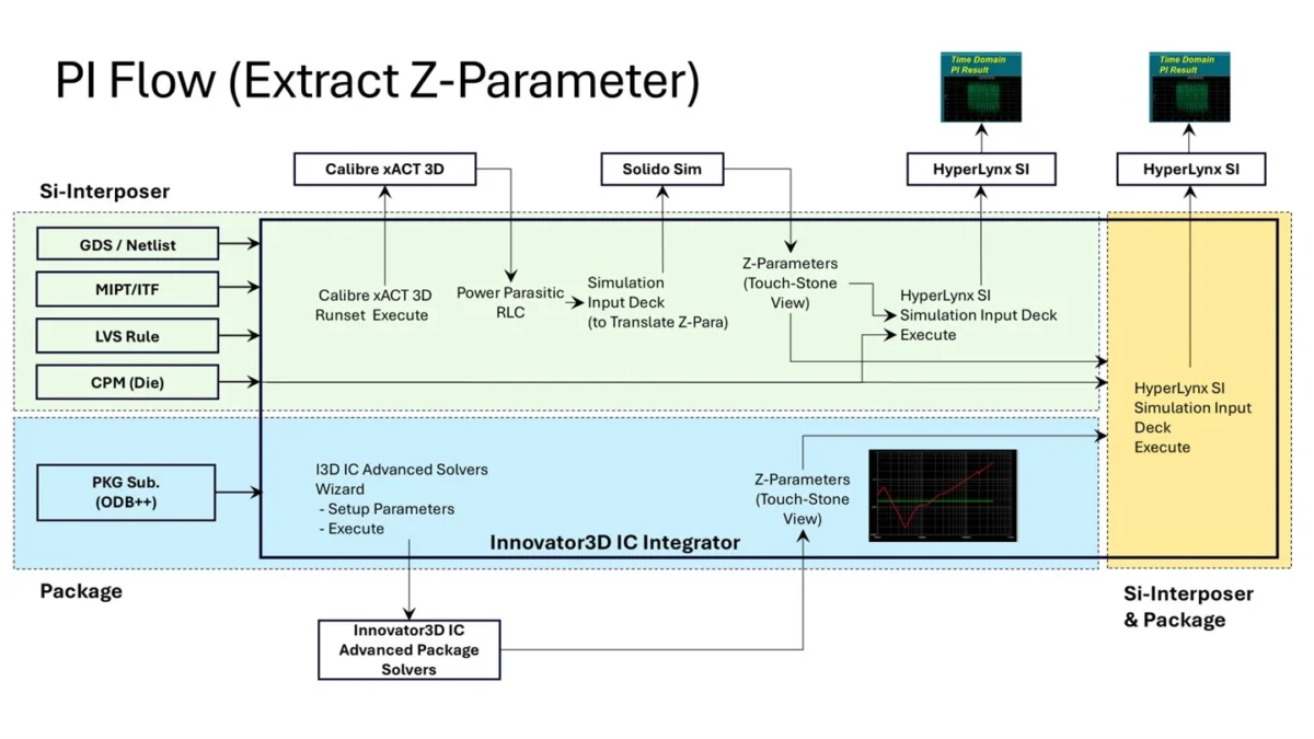
Siemens Innovator3D IC: A Unified System Cockpit
To bridge these gaps, the Siemens Innovator3D IC solution suite provides an integrated workflow that treats the entire 3D assembly as a single electrical entity. At the heart of this suite is the Innovator3D IC Integrator, which serves as a "central cockpit" for the design team. This tool consolidates all components—logic dies, High Bandwidth Memory (HBM) stacks, silicon interposers, and the final package—into a unified system model.
The Integrator acts as the single source of truth for the design. It ensures that electrical connectivity, power-domain definitions, and bump assignments are synchronized across all layers of the stack. By automating the orchestration of extraction and simulation, the suite allows engineers to perform "what-if" analyses early in the design phase. This "shift-left" strategy enables teams to identify potential resonance issues or excessive IR drops before the physical layout is finalized.
Technical Innovations in Modeling and Extraction
The effectiveness of the Siemens suite is rooted in three core technological pillars: die-level power modeling, high-fidelity TSV extraction, and broadband package analysis.
1. High-Fidelity Die-Level Modeling with mPower
Accurate system-level PI analysis is impossible without a realistic representation of how each die consumes power. Siemens mPower technology generates detailed Chip Power Models (CPMs). Unlike static models, these CPMs capture dynamic, workload-dependent switching behavior. This is crucial for simulating "worst-case" scenarios, such as when multiple processing cores switch simultaneously, creating a massive transient current demand ($di/dt$). These models are then seamlessly integrated into the broader system simulation to predict how die-level noise affects the rest of the stack.

2. Advanced TSV Extraction via Calibre xACT3D
TSVs are perhaps the most difficult structures to model in a 3D IC. Traditional electromagnetic solvers use surface meshing, which struggles with the cylindrical geometry of TSVs. This often results in an explosion of computational "unknowns," leading to prohibitively long simulation times or forced approximations that sacrifice accuracy.
Siemens’ Calibre xACT3D addresses this by employing cylindrical basis functions (specifically Bessel and Hankel functions) tailored to the geometry of the TSV. This mathematical approach allows the solver to capture complex electromagnetic interactions—including resistance, inductance, capacitance, and substrate coupling—with far fewer computational resources. This ensures that even designs with tens of thousands of TSVs can be extracted accurately and efficiently.
3. Broadband Electromagnetic Analysis with HyperLynx
The final piece of the puzzle is the package and interposer. These structures often contribute the majority of the PDN’s total impedance. Siemens uses Advanced Package Solvers to perform broadband EM extraction, modeling the package as a set of S-parameters. This allows the software to identify frequency-dependent behaviors, such as anti-resonance peaks. If the switching frequency of the silicon aligns with a resonance peak in the package, the resulting voltage noise can be amplified, leading to logic errors. HyperLynx SI/PI provides the simulation environment where these package models are stitched together with die and interposer models to create a complete, system-level electrical netlist.
Industry Context and Strategic Implications
The push toward 3D ICs is not merely a technical trend; it is a strategic necessity for the global semiconductor industry. As the cost per transistor in leading-edge nodes (3nm and beyond) continues to rise, "More than Moore" technologies—which focus on integration rather than just scaling—become the primary path for performance gains.

Market analysts suggest that the 3D IC market is poised for double-digit annual growth through the end of the decade. Companies like TSMC, Intel, and Samsung are investing billions in advanced packaging facilities (such as CoWoS and Foveros). However, the bottleneck for widespread adoption remains the complexity of the design and verification tools. By providing an automated, scalable flow, Siemens is lowering the barrier to entry for tier-2 and tier-3 chip designers who lack the massive internal R&D resources of the industry giants.
Furthermore, the reliability of 3D ICs is a major concern for mission-critical applications in automotive and aerospace. Power integrity is directly linked to long-term reliability; excessive noise can accelerate electromigration, leading to permanent circuit failure over time. A unified PI analysis flow provides the "sign-off confidence" required to deploy these advanced chips in vehicles and satellites.
Conclusion: Securing First-Pass Silicon Success
As 2.5D and 3D architectures become the standard for high-performance silicon, the margin for error in power delivery has effectively vanished. The traditional method of over-designing the PDN to compensate for uncertainty is no longer viable, as it wastes precious space and increases cost.
The Siemens Innovator3D IC solution suite represents a shift toward a more scientific, data-driven approach to power integrity. By unifying the design environment and employing advanced mathematical techniques for TSV and package modeling, Siemens allows engineering teams to de-risk their designs. In an industry where a single fabrication spin can cost tens of millions of dollars, the ability to predict and prevent power integrity failures at the system level is not just a technical advantage—it is a fundamental requirement for commercial success in the age of 3D integration. Through this holistic approach, Siemens is helping to ensure that the next generation of AI and HPC hardware is as reliable as it is powerful.
