
The semiconductor industry is currently navigating a paradigm shift as the design demands of modern system-on-chip (SoC) devices have surpassed the limits of manual intervention. As chips transition into the era of sub-5nm process nodes, the sheer volume of transistors and the intricate nature of multi-core environments have rendered traditional workflows obsolete. Today’s advanced SoCs are no longer mere collections of components; they are sprawling digital metropolises that require sophisticated, high-performance, and scalable automation to ensure that every internal element functions with perfect synchronicity. To maintain the pace of innovation, the industry is moving toward "generated architectures," where the integration of intellectual property (IP), hardware-software interfaces, and connectivity is handled by intelligent software platforms rather than human-led manual assembly.
The Escalating Crisis of SoC Complexity
At the heart of the modern electronics revolution is the SoC, a device that integrates all components of a computer or other electronic system into a single integrated circuit. A decade ago, an SoC might have contained a dozen IP blocks. Today, a high-end SoC for artificial intelligence (AI), mobile computing, or automotive applications can house hundreds or even thousands of IP blocks. These blocks—including central processing units (CPUs), graphics processing units (GPUs), neural processing units (NPUs), and complex memory controllers—are often sourced from a diverse array of third-party vendors or developed by specialized internal teams.
The integration challenge begins with the diversity of these IPs. Each functional block comes with its own set of specifications, communication protocols, and power requirements. Customizing these IPs is essential for differentiation; for instance, an NPU must be optimized to execute machine learning tasks at speeds significantly higher than traditional accelerators while maintaining a minimal power footprint. However, the process of gathering these disparate elements into a cohesive whole is fraught with risk. At advanced nodes, such as 3nm and 2nm, the industry is witnessing a shift where wire delay increasingly dominates gate delay. This means that the physical movement of data across the chip, rather than the computation itself, has become the primary bottleneck for performance and power efficiency.
The Hardware-Software Interface and the Single Source of Truth
One of the most critical points of failure in complex SoC design is the hardware-software interface (HSI). The HSI serves as the bridge between the physical hardware registers and the low-level software, including drivers and operating systems, that control them. Traditionally, register information was managed through fragmented documentation, spreadsheets, and separate files. As designs scale to billions of transistors, this manual approach leads to "mismatches" where the software team’s expectations do not align with the hardware’s actual implementation.
To resolve this, Arteris has introduced Magillem Registers, a tool designed to create a centralized representation of the HSI. This "single source of truth" is shared across hardware design, software development, verification, and documentation teams. By using a unified definition, the system can automatically generate the necessary artifacts, such as hardware register logic, software header files, and verification models. This automation ensures that when a hardware designer changes a register address, the update is instantly reflected in the software team’s files, eliminating weeks of manual reconciliation and debugging.
The economic impact of these mismatches is substantial. Industry data suggests that a single "spin" or redesign of an advanced node SoC can cost a company upwards of $50 million to $100 million. By automating the HSI, companies can significantly reduce the risk of functional errors that lead to such costly delays.

Streamlining IP Packaging for Global Reuse
As semiconductor firms expand their portfolios, the ability to reuse IP across different chip designs becomes a competitive necessity. However, IP blocks from different sources often use varying conventions and documentation styles. Magillem Packaging addresses this by capturing interface definitions, configuration parameters, and memory map intent in a consistent representation.
This systematic approach allows IP to be integrated into new designs without the need for engineers to re-derive details from source code or outdated documentation. In a globalized design environment where teams in different time zones may be working on the same project, having a standardized packaging format reduces the "integration tax"—the time and effort spent simply making things fit together rather than innovating on the core architecture.
From Simple Interconnects to Automated Network-on-Chip (NoC)
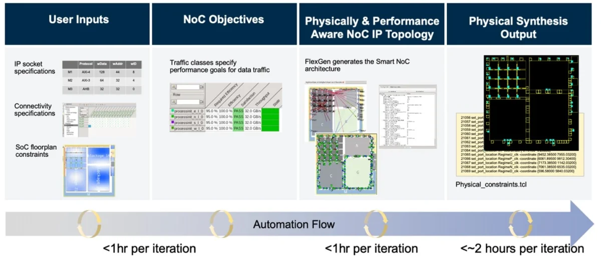
Perhaps the most significant evolution in SoC design is the transition from simple connectivity fabrics to sophisticated Network-on-Chip (NoC) architectures. In the past, data movement was handled by relatively simple buses or crossbars. In a modern SoC with thousands of endpoints, the interconnect has become the "central nervous system" of the device.
The role of the interconnect has shifted from simple connectivity to a system-level architectural element that must manage traffic behavior, latency targets, and bandwidth distribution while accounting for physical constraints like floorplanning. Manual design of these interconnects has become an impossible task. Iterative refinement—where a designer tweaks a wire and then re-runs a simulation—is now a major bottleneck in the development cycle.
To address this, Arteris developed FlexGen, a technology that automates the generation of optimized system connectivity. Unlike traditional approaches where the interconnect is configured after the IPs are integrated, FlexGen uses system-level inputs—such as IP characteristics, traffic requirements, and physical constraints—to synthesize an architecture from the ground up. This shift from manual configuration to automated generation allows the NoC to be tailored to the specific needs of the SoC, including topology selection and resource allocation. Because FlexGen operates on the same consistent inputs used by the Magillem suite, the generated interconnect is inherently aligned with the hardware-software interface and the IP packaging.
Chronology of SoC Integration Evolution
The path to automated SoC integration has followed a distinct chronological progression:
- 1990s – The Era of Discrete Components: Systems were built using multiple chips on a printed circuit board. Integration was handled at the board level.
- Early 2000s – Rise of the SoC: The first true SoCs appeared, integrating a CPU and basic peripherals. Manual bus design (like early AMBA protocols) was sufficient.
- 2010s – The IP Explosion: The smartphone era demanded massive integration. The "IP-XACT" standard was popularized to help describe IP blocks, and the first commercial NoCs began to replace traditional buses.
- 2020s – The AI and Chiplet Era: Integration has become "architecture." Automation tools like FlexGen and Magillem are now required to manage the complexity of billions of transistors and the transition toward chiplet-based designs, where multiple dies are integrated into a single package.
Supporting Data and Market Impact
The shift toward automated SoC integration is reflected in market trends. According to industry analysts, the global SoC market is projected to reach over $200 billion by 2027, driven by the demand for AI, 5G, and autonomous driving. Within this market, the cost of design is rising faster than the revenue generated by the chips themselves.

Data from International Business Strategies (IBS) indicates that the design cost for a 3nm chip can exceed $600 million. Of that cost, integration and verification account for approximately 60-70%. By adopting automated flows that reduce manual labor and the likelihood of errors, semiconductor companies can theoretically reclaim 20-30% of their development schedule, providing a massive advantage in the race to market.
Official Responses and Strategic Implications
While Arteris has not issued a formal press release for this specific synthesis of technologies, the company’s leadership has frequently emphasized the "system-level discipline" required for modern design. Industry experts suggest that the move toward generated architectures is a direct response to the "labor crisis" in the semiconductor industry. There simply are not enough expert RTL (Register Transfer Level) designers to manually integrate the next generation of chips.
"The industry is reaching a point where you cannot throw more engineers at the problem," says a senior analyst in the EDA (Electronic Design Automation) space. "You have to change the methodology. Arteris is essentially providing a way to codify the expertise of an architect into an automated toolset."
The Broader Impact: Toward a Software-Defined Hardware Future
The implications of this shift extend far beyond the engineering department. As integration becomes a structured and repeatable process, SoC teams can shift their focus away from "implementation complexity" and toward "architectural differentiation."
In the automotive sector, this means faster development of ADAS (Advanced Driver Assistance Systems) that can process sensor data with lower latency. In the data center, it allows for the rapid creation of custom AI accelerators tailored to specific large language models (LLMs).
Furthermore, this automated approach is a prerequisite for the burgeoning chiplet market. As the industry moves away from monolithic dies toward "systems-in-package," the need for a unified, automated way to manage interfaces and connectivity across multiple pieces of silicon becomes even more critical. Arteris’ approach provides the foundation for this multi-die future, ensuring that the same "single source of truth" used for a single chip can eventually span an entire ecosystem of chiplets.
Conclusion
The transition from manual workflows to generated architectures marks the end of the "artisanal" era of chip design. By integrating Magillem Registers, Magillem Packaging, and FlexGen into a unified system-level approach, Arteris is providing the tools necessary to navigate the extreme complexity of modern SoCs. This methodology ensures that system intent is consistently applied across hardware, software, and connectivity, resulting in improved predictability and a significant reduction in development effort. As the semiconductor industry continues to push the boundaries of physics and scale, the ability to automate the integration of billions of transistors will be the defining factor in the success of the next generation of digital innovation.
