
The semiconductor industry is currently navigating a pivotal transition as chip designs migrate toward deep submicron nodes, specifically the 3nm and 2nm regimes. As transistor densities increase and operating voltages decrease to conserve power, the sensitivity of these devices to electrical noise has reached a critical threshold. At the heart of this challenge lies the clock network—the fundamental "heartbeat" of a digital system. Ensuring that clock signals remain pristine across massive, multi-billion transistor integrated circuits (ICs) has become a primary bottleneck in modern electronic design automation (EDA) workflows. Traditional simulation methodologies, which once sufficed for older process nodes, are increasingly proving inadequate, lacking the granularity to understand complex clocking requirements or the capacity to simulate the full clock network of a large-scale System-on-Chip (SoC).
The Escalating Crisis of Clock Signal Integrity
In high-performance computing (HPC), artificial intelligence (AI), and advanced automotive electronics, chips are frequently required to operate at frequencies exceeding 1 GHz while utilizing ultra-low voltage rails. This combination creates a perfect storm for signal degradation. Clock signal integrity (SI) and clock jitter are no longer secondary concerns; they are now primary causes of silicon failure and expensive re-spins.
Clock jitter—the deviation of a clock edge from its ideal position in time—is primarily driven by noise within the power delivery network (PDN). When thousands of gates switch simultaneously, they draw current that causes local voltage fluctuations. These fluctuations, in turn, alter the propagation delay of clock buffers. The resulting timing variation can lead to catastrophic failures, including metastability, where a flip-flop fails to settle into a stable state, and race conditions, where data arrives before or after its intended window.

Furthermore, the degradation of clock signals often leads to a reduction in the maximum operating frequency (Fmax). For a commercial product, a lower Fmax translates directly to reduced performance and diminished market competitiveness. Traditional SPICE (Simulation Program with Integrated Circuit Emphasis) simulations, while accurate, are computationally expensive. Attempting to run a SPICE-level analysis on a modern clock tree can take weeks, making it impossible to perform the iterative debugging required during the engineering change order (ECO) or signoff stages of design.
The Technical Limitations of Legacy Simulation Tools
For decades, engineers relied on general-purpose circuit simulators to verify timing. However, these tools were not designed for the sheer scale of contemporary SoCs. A typical modern processor may contain hundreds of millions of transistors dedicated solely to the clock distribution network. General simulators struggle with "subtle understanding," failing to recognize the specific failure mechanisms unique to clock trees, such as duty-cycle distortion (DCD) and rail-to-rail (RTR) swing failures.
When simulations run for days, the design cycle slows down, and engineers are forced to make conservative "guard band" assumptions. These margins—extra time added to account for uncertainty—effectively waste the performance gains promised by advanced 3nm or 5nm process nodes. To reclaim this lost performance, the industry has shifted toward dedicated clock analysis solutions that offer the accuracy of SPICE with the throughput of static timing analysis (STA).
Synopsys PrimeClock: A Paradigm Shift in Clock Analysis
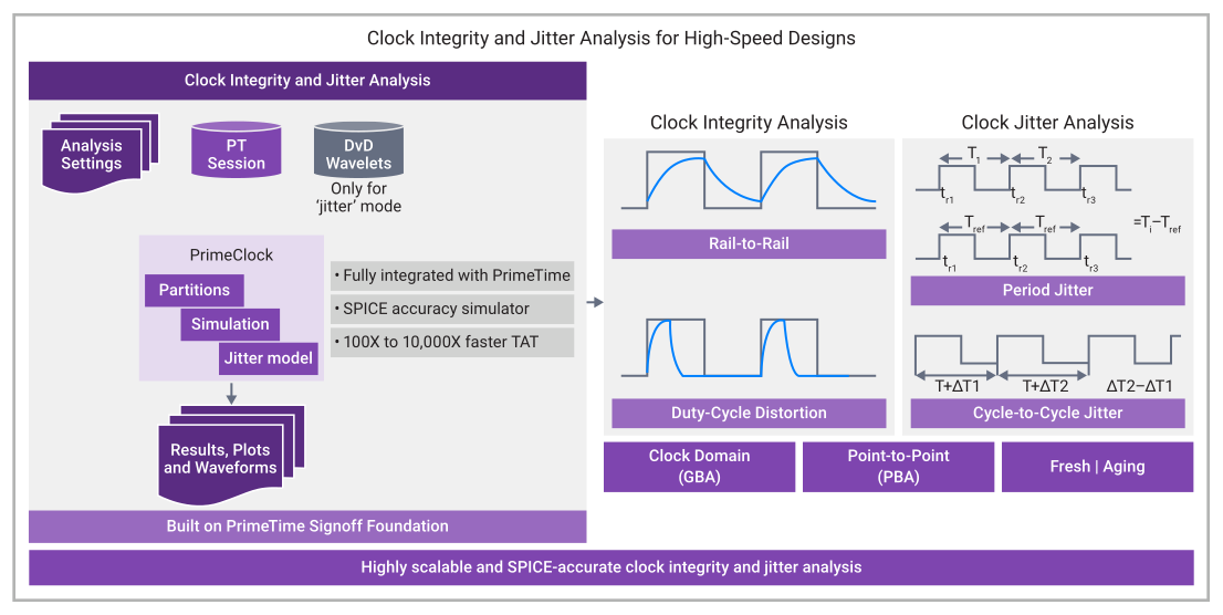
To address these systemic challenges, Synopsys introduced PrimeClock, a dedicated solution designed to bridge the gap between slow, high-accuracy circuit simulation and fast, but often overly optimistic, static timing tools. PrimeClock is engineered to handle both tree and mesh clock networks at the block, subsystem, and full-chip levels.

The core innovation of PrimeClock lies in its scalable partitioning and distributed simulation architecture. By breaking down a massive clock network into manageable segments and analyzing them in parallel, the tool achieves a turnaround time (TAT) that is 100X to 1000X faster than traditional circuit simulators. Despite this speed, it maintains SPICE-level accuracy through tight integration with existing circuit simulation engines.
Key Capabilities and Failure Mechanism Detection
PrimeClock focuses on four critical failure mechanisms that are often missed by standard STA tools:
- Rail-to-Rail (RTR) Failures: The tool checks for full voltage swing on all clock pins. If a signal does not reach the required voltage levels, it can lead to intermittent switching or increased sensitivity to noise.
- Duty-Cycle Distortion (DCD): PrimeClock monitors the symmetry of the clock signal. An uneven duty cycle shrinks the available timing margin for half-cycle paths, a common issue in high-speed DDR memory interfaces and AI accelerators.
- Period Jitter: This measures the deviation of individual clock periods.
- Cycle-to-Cycle (C2C) Jitter: This tracks the change in period between adjacent cycles, which is vital for maintaining the stability of phase-locked loops (PLLs).
Chronology of Adoption and Industry Validation
The emergence of PrimeClock as a standard in the EDA toolchain has been marked by significant milestones at major industry conferences. These events provide a timeline of how the tool has moved from a specialized solution to a mainstream requirement for advanced node design.
SNUG Silicon Valley 2025: Arm’s Breakthrough
At the Synopsys Users Group (SNUG) event in 2025, Arm, a global leader in semiconductor IP, presented a landmark case study. Arm engineers reported utilizing PrimeClock to analyze a design containing 100 million transistors. Historically, such a task would have been prohibitive in terms of time and compute resources. Using the tool’s distributed analysis capabilities, Arm completed the full clock integrity analysis in just two hours. More importantly, the analysis identified "structurally weak" clock nodes that had gone undetected by other tools. By fixing these vulnerabilities before fabrication, Arm avoided potential silicon failures and ensured the robustness of their high-performance cores.

Synopsys Converge 2026: Socionext and 3nm Scaling
A year later, at the Synopsys Converge Conference 2026, Socionext shared results from their work on a large-scale AI and HPC design based on a 3nm process. For Socionext, the challenge was timing closure on an incredibly dense SoC. By integrating PrimeClock into their operational flow, they achieved a 40% reduction in DCD runtime. The ability to quickly identify and resolve duty-cycle issues allowed their team to reach timing convergence much faster, significantly shortening the overall time-to-market.
Advanced Modeling: Machine Learning and Aging
As semiconductor devices age, their electrical characteristics shift due to phenomena such as Bias Temperature Instability (BTI) and Electromigration (EM). A clock network that passes timing on "Day 1" might fail after two years of operation in a data center or an autonomous vehicle. PrimeClock addresses this by modeling aging stress conditions, allowing designers to simulate "fresh" versus "aged" silicon.
Furthermore, Synopsys has integrated machine learning (ML) driven models into the jitter analysis flow. These ML models are trained to predict how dynamic voltage drops (DVD) will affect clock timing. By using ML wavelets—often generated in conjunction with Synopsys RedHawk-SC—the tool can predict jitter impacts with extreme precision without needing to re-simulate every possible switching scenario. This ML-driven approach is cited as a primary factor in the 1000X speedup observed in jitter analysis.
Broader Impact and Implications for the Semiconductor Ecosystem
The shift toward dedicated clock analysis tools like PrimeClock reflects a broader trend in the electronics industry: the move away from "one-size-fits-all" verification. As designs become more heterogeneous—incorporating CPUs, GPUs, and specialized AI tiles on a single die—the complexity of the clocking scheme grows exponentially.

Impact on AI and High-Performance Computing
In the AI sector, where massive parallel processing is the norm, even a slight misalignment in clock signals across a chip can lead to data corruption or reduced throughput. PrimeClock’s ability to provide path-based analysis of point-to-point paths ensures that the high-speed data buses required for AI training remain synchronized.
Automotive and Safety-Critical Systems
For the automotive industry, the implications are even more profound. As vehicles move toward Level 4 and Level 5 autonomy, the reliability of the underlying silicon is a matter of public safety. The ability to model aging and ensure clock integrity over a 15-year vehicle lifespan is no longer an optional feature; it is a regulatory and functional necessity.
Conclusion: The New Standard for Signoff
The integration of Synopsys PrimeClock into the design flow represents a necessary evolution in semiconductor engineering. By providing a bridge between the physical realities of deep submicron electronics and the need for rapid digital design cycles, it enables the creation of faster, more reliable, and more efficient chips.
The data from industry leaders like Arm and Socionext confirms that the benefits of this technology—ranging from 100X faster turnaround times to a 40% reduction in runtime for specific violations—are transformative. As the industry looks toward the sub-2nm era, the role of specialized, SPICE-accurate clock analysis will only become more central to the success of global semiconductor manufacturing. For developers pushing the boundaries of what is possible in silicon, the transition from traditional simulation to dedicated clock integrity analysis is not merely an upgrade; it is a prerequisite for the next generation of technological innovation.
