
The semiconductor industry has entered a transformative era in 2026, characterized by the shift from traditional automated tools to autonomous "agentic" AI systems that manage the complexities of chip design and system orchestration. This evolution was highlighted during the recent CadenceLive Silicon Valley event, where industry leaders showcased how the convergence of generative AI, physics-based simulation, and custom silicon is redefining the limits of Moore’s Law. As the industry grapples with the demands of massive-scale AI infrastructure, companies like Meta, Nvidia, and Infineon are pivoting toward integrated ecosystems that prioritize energy efficiency, data-centric architectures, and a robust talent pipeline.
The Rise of Agentic AI in Electronic Design Automation
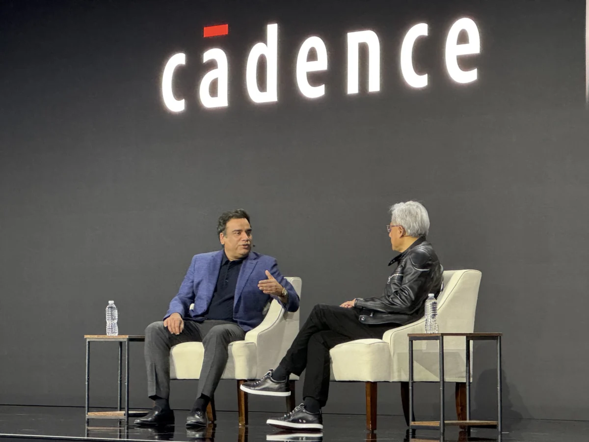
A primary focus of the mid-2026 technological cycle is the deployment of "agentic AI" within Electronic Design Automation (EDA). Cadence has significantly expanded its ChipStack portfolio, introducing a "head agent" designed to orchestrate the multifaceted aspects of semiconductor and system design. Unlike previous iterations of AI in EDA, which focused on specific optimization tasks, these new agents are capable of making high-level design decisions across custom, analog, and digital implementation sectors.
The collaboration between Cadence and Nvidia represents a strategic move to combine agentic AI with digital twins and physics-based simulations. By utilizing Nvidia’s accelerated computing platforms, Cadence aims to create a closed-loop environment where AI agents can predict physical outcomes of chip designs before they reach the manufacturing stage. Simultaneously, a partnership with Google has integrated Cadence’s "Super Agent" with the Gemini model on Google Cloud, providing designers with a scalable, cloud-native environment for high-performance computing (HPC) workloads. This integration is expected to reduce the time-to-market for complex systems-on-chip (SoCs) by automating signoff and verification processes that previously required months of manual oversight.
The Stanford 2026 AI Index Report corroborates this trend, noting a sharp inflection point in AI capability. The data suggests that as AI models become more adept at specialized engineering tasks, the productivity of semiconductor design teams has the potential to increase by orders of magnitude, provided the underlying hardware can support the requisite computational intensity.

Custom Silicon and Large-Scale AI Infrastructure
In the realm of hardware, Meta has unveiled the second generation of its Meta Training and Inference Accelerator (MTIA), a custom chip specifically engineered for the company’s internal large-scale AI infrastructure. This development marks a significant milestone in Meta’s long-term strategy to reduce its reliance on general-purpose GPUs and optimize its data centers for specific social media and AI workloads.
To ensure the scalability of this project, Meta has entered a multi-generational partnership with Broadcom. The collaboration focuses on co-developing custom AI silicon and deploying over one gigawatt (1GW) of capacity through Broadcom’s XPU platform and advanced Ethernet technologies. This massive deployment underscores the industry’s shift toward high-speed interconnects and specialized silicon as the primary bottlenecks for AI training. The move also signals a broader trend where hyperscalers are increasingly acting as semiconductor architects, designing bespoke hardware that maximizes performance-per-watt in the data center.
Complementing these advancements in logic are breakthroughs in interconnect technology. Panmnesia recently announced the sampling of a PCIe 6.4-CXL 3.2 fusion switch chip. This technology is critical for memory pooling and expansion, allowing data centers to share memory resources more efficiently across different processing units. As AI models grow in size, the ability to move data with minimal latency—supported by UALink and Ethernet-based interconnects—has become as vital as the raw processing power of the chips themselves.
Automotive Semiconductors and the Data-First Architecture
The automotive sector remains a dominant force in the semiconductor market, with Infineon maintaining its position as the top global supplier. According to 2025 market data, Infineon holds a 13% share of the overall automotive semiconductor market and a commanding 36% share of the microcontroller unit (MCU) segment. The company’s influence extends beyond terrestrial applications, as its radiation-hardened solutions were recently utilized in NASA’s Artemis II mission, demonstrating the high reliability required for modern silicon.
A significant structural shift is occurring in how vehicles handle information. The Automotive Edge Computing Consortium (AECC) has introduced a "data-first" architecture designed to manage the massive influx of information generated by autonomous and software-defined vehicles. This architecture utilizes a distributed, tiered model that processes data across vehicles, edge infrastructure, and cloud platforms. By combining cellular, Wi-Fi, and inter-vehicle data transfer, the AECC aims to provide a scalable framework for future automotive services.

Strategic partnerships are also accelerating the transition to centralized vehicle architectures. Bosch and Qualcomm have expanded their collaboration to focus on Advanced Driver Assistance Systems (ADAS) and emerging "zonal" computing models. Meanwhile, imec’s Automotive Chiplet Program (ACP) has gained momentum with the addition of Silicon Box as a partner. This initiative explores the use of chiplets—smaller, modular pieces of silicon—to create high-performance automotive processors that are easier to manufacture and more cost-effective than traditional monolithic designs.
Quantum Computing and Advanced Materials Research
Research and development in 2026 are pushing the boundaries of traditional physics. DARPA has launched the Heterogeneous Architectures for Quantum (HAQ) program, which seeks to integrate different types of qubits—the fundamental units of quantum information—into a single system. By combining the unique strengths of various qubit technologies, DARPA hopes to overcome the scaling and error-correction hurdles that have historically hindered quantum computing.
In the field of materials science, a UCLA-led research team has discovered that metallic theta-phase tantalum nitride exhibits thermal conductivity nearly three times higher than copper or silver. This discovery has profound implications for the semiconductor industry, where heat dissipation is a primary limiting factor for chip performance. Utilizing such materials in future packaging could allow for denser, more powerful processors without the risk of thermal failure.
Space exploration is also driving silicon innovation. NASA has selected Synopsys and Electro Magnetic Applications to research the effects of the lunar environment on the Artemis program’s spacesuits and communication systems. The research focuses on triboelectrification and electrostatic discharge, ensuring that the electronic components within spacesuits can withstand the harsh electrical conditions of the Moon’s surface.
Workforce Development and the Talent Pipeline
As the semiconductor industry expands, the need for a skilled workforce has led to significant investments in education and vocational training. In Phoenix, Arizona—a burgeoning hub for chip manufacturing—a local school district has unveiled a 16,500-square-foot cleanroom environment. This facility allows high school students to gain hands-on experience in fab operations and robotics, directly preparing them for roles in the nearby facilities operated by industry giants.

Similarly, the Oregon government has awarded over $8.5 million in grants to bolster the state’s semiconductor talent pipeline. These funds support various initiatives, including the construction of mock fab rooms and the creation of internship programs that bridge the gap between secondary education and professional careers. On an international scale, Mitsubishi Chemical, PsiQuantum, and the University of Tokyo have formed a coalition to train Japan’s quantum workforce, reflecting the global nature of the competition for high-tech talent.
Security Challenges and Regulatory Oversight
The rapid advancement of technology has brought new security challenges to the forefront. The Federal Communications Commission (FCC) has proposed new classifications for consumer routers manufactured abroad, labeling them as potential security risks. A report from the Global Electronics Association suggests that these restrictions could lead to increased costs and slower adoption of the latest Wi-Fi standards. However, some manufacturers, such as Netgear, have already secured conditional exemptions, highlighting the complex interplay between national security and the global supply chain.
On the technical side, the National Institute of Standards and Technology (NIST) is developing new methods to improve the resilience of bus-connected hardware. By repurposing component firmware as a "network of forensic units," NIST aims to create a more robust monitoring system that can detect and mitigate hardware-level security breaches in real-time.
Broader Impact and Industry Implications
The developments of early 2026 suggest a semiconductor industry that is no longer focused solely on shrinking transistors. Instead, the focus has shifted toward "system-level" innovation. The integration of agentic AI into design workflows, the rise of custom hyperscale silicon, and the move toward chiplet-based architectures in the automotive sector all point to a more modular and intelligent approach to computing.
As companies prepare for a heavy schedule of industry events throughout the second quarter of 2026—including the TSMC Technology Symposium, Display Week, and the Electronic Components and Technology Conference (ECTC)—the industry remains focused on balancing performance with power efficiency. The transition to curvilinear masks, the adoption of 2.5D packaging for AI applications (as seen with Onto Innovation’s Dragonfly G5), and the exploration of quantum-classical hybrid systems are all part of a broader effort to sustain the pace of technological progress in a post-Moore’s Law world. The successful navigation of these trends will depend not only on technical ingenuity but also on the industry’s ability to cultivate a new generation of engineers capable of managing the increasingly autonomous tools that define the modern silicon landscape.
