
The global semiconductor industry is currently undergoing a period of profound structural transformation, driven by the escalating demands of artificial intelligence (AI), the necessity for more efficient power management, and a strategic push toward regional supply chain resilience. Recent developments across manufacturing, research, and corporate leadership underscore a shift away from traditional monolithic scaling toward heterogeneous integration and advanced packaging. From Apple’s strategic pivot to diversify its supply chain beyond its long-standing reliance on TSMC to GlobalFoundries’ unveiling of advanced co-packaged optics (CPO) solutions, the sector is reacting to the dual pressures of physical limits in chip design and the urgent need for massive data throughput in hyperscale data centers.
Manufacturing and Global Supply Chain Shifts
A significant development in the manufacturing sector is the establishment of a new advanced packaging site in Taiwan. As Moore’s Law slows, the industry has turned to "More than Moore" strategies, where the focus shifts from shrinking transistors to how chips are assembled. Advanced packaging techniques, such as 2.5D and 3D integration, allow different types of silicon—such as processors and high-bandwidth memory (HBM)—to be placed closer together, reducing latency and power consumption. This new site in Taiwan is expected to bolster the island’s position as a hub for Outsourced Semiconductor Assembly and Test (OSAT) services, providing essential capacity for the next generation of AI accelerators.
In a move that has sent ripples through the ecosystem, Apple is reportedly looking beyond TSMC for certain aspects of its future hardware production. While TSMC remains the primary foundry for Apple’s silicon, the tech giant is exploring alternative partners for specialized components and advanced packaging. This shift reflects a broader industry trend toward "multi-sourcing" to mitigate geopolitical risks and ensure supply stability. Historically, Apple’s lead-customer status at TSMC has given it first access to cutting-edge nodes like 3nm; however, the complexity of future 2nm and 1.4nm processes, combined with the need for massive volumes, is forcing even the largest players to reconsider their dependency on a single manufacturer.
Simultaneously, the production of critical raw materials like gallium is receiving renewed attention. Gallium is essential for gallium nitride (GaN) semiconductors, which are increasingly used in power electronics for electric vehicles (EVs) and 5G infrastructure. With global supply chains under scrutiny due to export controls and trade tensions, Western firms are seeking to diversify gallium sourcing to ensure that the transition to green energy and high-speed communications is not bottlenecked by material shortages.

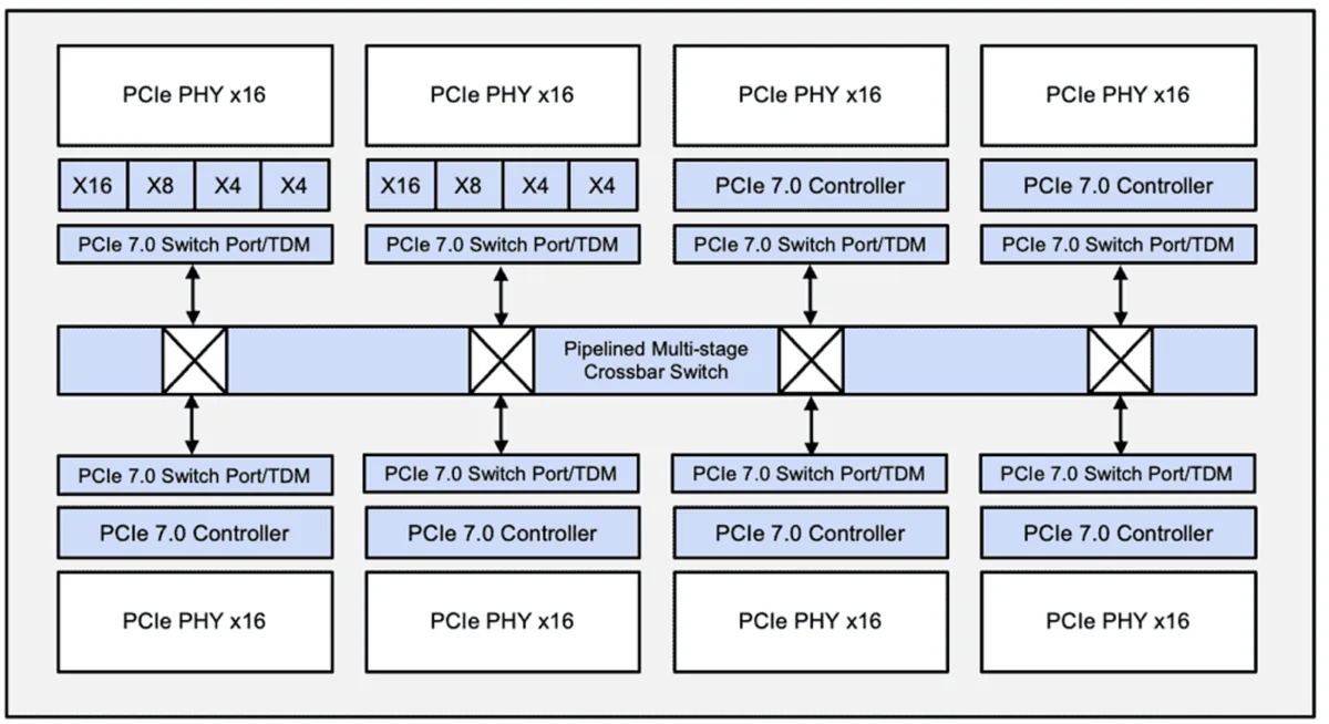
Breakthroughs in High-Performance Computing and Data Transfer
As data centers evolve to handle generative AI workloads, the bottleneck has shifted from raw compute power to data movement. GlobalFoundries (GF) has addressed this with its latest Co-Packaged Optics (CPO) solution. Traditional copper interconnects struggle with the bandwidth requirements of modern AI clusters and consume significant amounts of power. GF’s solution integrates silicon photonics directly into the chip package, allowing for optical data transfer. This innovation significantly reduces power consumption while increasing the distance and speed at which data can travel between GPUs and memory.
In the realm of interface standards, the development of PCIe 7.0 tools marks a critical milestone. Rambus recently showcased its PCIe 7.0 switch IP, which utilizes time-division multiplexing to manage data flow. The PCIe 7.0 standard is designed to deliver a raw bit rate of 128 GT/s per lane, doubling the bandwidth of PCIe 6.0. This is vital for the next generation of AI servers, where the throughput between the CPU, GPU, and storage must be maximized to prevent "starvation" of the processing units.
Supporting these high-speed environments, SiTime has launched its Elite 2 Super-TCXO (Temperature-Compensated Crystal Oscillator). In the high-heat environment of an AI data center, timing precision is easily disrupted. SiTime’s new oscillator provides the stability required to keep GPUs synchronized, which directly improves utilization rates. Even a microsecond of drift in timing can lead to data errors or system stalls in distributed AI training, making high-precision timing a foundational element of modern compute architecture.
Innovations in Integrated Circuits and Materials Science
The research sector continues to push the boundaries of what is possible at the chip level. A team at the University of Southern California (USC) has developed a framework for designing Radio Frequency Integrated Circuits (RFICs) using metaheuristic algorithms. These algorithms explore vast design spaces through guided randomness, discovering novel chip architectures that human engineers might never have conceived. This "AI for Silicon" approach is becoming essential as chip designs become too complex for traditional manual layout methods.
In Germany, Fraunhofer IZM has achieved a breakthrough in power electronics by creating a 99% efficient inverter. The unit can handle 500 kilowatts of power while occupying a volume of only one liter. This level of power density is unprecedented and has significant implications for the EV industry, where reducing the weight and size of power electronics directly translates to increased vehicle range and efficiency.

In the United States, researchers at Argonne National Laboratory and Northwestern University are collaborating on "superconductors by design." By understanding and controlling how atomic structures form, they are predicting new materials that could revolutionize quantum hardware. This research is supported by a surge in quantum hardware funding, as governments and private investors race to realize the potential of quantum computing for cryptography, material discovery, and complex optimization.
Workforce Development and Educational Initiatives
The semiconductor industry faces a daunting talent gap. In the United States alone, reports suggest a shortage of tens of thousands of skilled workers by the end of the decade. To combat this, Stony Brook University has launched an NSF-supported program to train students in semiconductor and advanced nanomanufacturing skills. The program emphasizes paid hands-on experience and involves collaborations with the Brookhaven National Laboratory and industry giants like GlobalFoundries and Wolfspeed.
Similarly, the University of Sheffield recently hosted the "UK Tiny Tapeout" workshop, where over 120 students designed and submitted their own chips for fabrication. This hands-on approach is designed to demystify chip design and encourage a new generation of engineers to enter the field. Purdue University is also contributing to this effort with its "Building the U.S. Semiconductor Workforce" webinar series, aimed at connecting students with career opportunities in microelectronics, particularly in light of the funding provided by the CHIPS and Science Act.
Corporate Leadership and Strategic Governance
The leadership landscape is also shifting as legacy companies pivot toward AI and high-performance computing (HPC). Intel recently announced key executive appointments, naming Pushkar Ranade as Chief Technology Officer and Alex Katouzian as Executive Vice President and General Manager of Client Computing & Physical AI. These moves signal Intel’s commitment to integrating AI capabilities directly into consumer hardware—a trend often referred to as "AI at the Edge."
In the public sector, the Lawrence Berkeley National Laboratory has named Katherine Yelick as its next director. With her extensive background in HPC and AI, Yelick is expected to lead the lab’s efforts in utilizing supercomputing to solve global challenges in climate science and energy. Her appointment underscores the growing intersection between national security, scientific research, and advanced semiconductor technology.

Security, Reliability, and Environmental Impact
As AI becomes more integrated into critical infrastructure, security warnings are increasing. Industry experts are highlighting the vulnerabilities of AI models to adversarial attacks and the potential for "backdoors" in hardware. This has led to a renewed focus on "Secure by Design" principles, where security is integrated at the architectural level rather than added as an afterthought.
Furthermore, the environmental impact of the semiconductor lifecycle remains a topic of intense study. Recent reports have analyzed the impact of temperature on EV batteries, noting that extreme heat or cold can significantly degrade performance and lifespan. As the industry moves toward more powerful chips and larger battery packs, managing the thermal envelope of electronics—from data centers to vehicles—has become a primary engineering challenge.
Broader Industry Implications and Future Outlook
The convergence of these developments indicates a semiconductor industry that is no longer solely focused on miniaturization. Instead, the focus is on systemic efficiency. The transition to PCIe 7.0, the adoption of CPO, and the rise of advanced packaging all point to a future where the "package" is just as important as the "chip."
The industry is also becoming increasingly localized. The establishment of new sites in Taiwan, the workforce initiatives in the US and UK, and the European Union’s efforts to map its chip companies all reflect a desire for regional autonomy. However, the global nature of the supply chain—from gallium mining to OSAT services—means that total independence is unlikely. Instead, the industry is moving toward a model of "trusted partnerships" and diversified risk.
As the sector moves into the mid-2020s, the primary challenge will be balancing the insatiable demand for AI compute with the physical realities of power consumption, thermal management, and workforce availability. The innovations highlighted this week—from MIT’s lidar chips to SiTime’s oscillators—are the building blocks of a new electronic era that is smarter, faster, and more integrated than ever before.
