
The semiconductor industry is currently undergoing one of its most significant structural transformations since the invention of the integrated circuit. As the physical limits of monolithic System-on-Chip (SoC) scaling become increasingly apparent, the move toward chiplets and multi-die systems is fundamentally altering the methodologies used to build high-performance silicon. This shift is not merely an architectural change; it is forcing a comprehensive redesign of the engineering workflows that have governed chip manufacturing for decades. In the era of planar SoCs, design challenges generally concluded at the edge of a single die. Today, in a landscape dominated by 2.5D and 3D architectures, performance, reliability, and yield are dictated by how multiple dies interact within an advanced package, how data moves across complex interconnects, and how various physical forces—thermal, mechanical, and electrical—behave in tandem.
The Breakdown of Linear Design Methodologies
For years, the semiconductor design flow was largely linear. Architects defined the system, logic designers created the RTL, verification teams checked the code, and physical designers handled the layout. Packaging was often treated as an afterthought—a mechanical enclosure designed to protect the silicon and provide connectivity to the printed circuit board (PCB). However, experts across the Electronic Design Automation (EDA) and Intellectual Property (IP) sectors agree that this siloed approach is no longer viable.
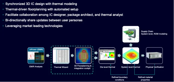
Andras Vass-Vernai, a 3D-IC solution architect for thermal management and reliability at Siemens EDA, observes that the complexity of advanced packaging has necessitated a cultural shift within engineering teams. Historically, mechanical engineers managed thermal issues in isolation, often trading specifications with electrical designers without real-time collaboration. This "siloed" method worked for gadgets and mobile phones where miniaturization was the primary goal, but the high-density integration of 2.5D and 3D systems has made early-stage decision-making critical. In the modern workflow, a decision made during the architectural phase regarding die placement can have catastrophic thermal or mechanical consequences during assembly, making it essential to connect modeling and manufacturing analysis much earlier in the cycle.
The Multi-Physics Challenge in 3D Integration
The transition from a monolithic "2D" view of ASIC design to a layered "2.5D or 3D" perspective introduces what engineers call a multi-physics problem. Prem Theivendran, director of software engineering at Expedera, notes that the majority of modern design "nightmares" stem from interconnects. When multiple dies are stacked or placed side-by-side on an interposer, designers must contend with a convergence of electrical, thermal, and mechanical issues.
Unlike a single chip, where heat dissipates relatively predictably, stacked dies create internal heat traps. As temperatures rise, leakage power increases, which in turn raises the total temperature of the system. This thermal expansion can lead to "warpage" or mechanical stress, potentially snapping the microscopic solder bumps that connect the dies. Furthermore, higher temperatures increase signal delay, complicating timing closure. This interdependence means that signal integrity, power integrity, thermal management, and mechanical stability must be analyzed simultaneously rather than sequentially.
The move toward open ecosystems and standards like Universal Chiplet Interconnect Express (UCIe) has further complicated this landscape. Traditionally, a company might design every component of an SoC in-house using proprietary interfaces. In the chiplet era, a single package might contain a processor from one vendor, an I/O chiplet from another, and specialized AI accelerators from a third. Ensuring that these disparate components—each with their own thermal profiles and power requirements—work together seamlessly requires a unified workflow that transcends the traditional boundaries of the chip.
Chronology of the Shift: From Monolithic to Modular
The move toward chiplets has followed a clear chronological progression over the last decade.
- The Monolithic Era (Pre-2015): Scaling was driven primarily by Moore’s Law. Performance gains were achieved by shrinking transistors on a single die.
- The Rise of 2.5D (2015–2020): High-bandwidth memory (HBM) and the use of silicon interposers began to gain traction, particularly in data center GPUs. This period saw the first widespread adoption of multi-die integration for high-performance computing.
- The Chiplet Standard Era (2020–Present): The formation of the UCIe consortium and the emergence of advanced packaging technologies like hybrid bonding have moved chiplets from a niche solution to the industry standard for AI and high-performance computing (HPC).
This timeline reflects a shift in the "boundary of concern." As Long Thanh (Kevin) Bui, AMS senior manager at Mixel (a Silvaco company), points out, the focus has moved from what happens inside the chip to what happens at the interface between chips. In a traditional design, a localized defect results in the loss of one die. In a chiplet-based system, a single failed interconnect or a defective I/O chiplet can ruin a fully assembled package costing thousands of dollars.

Essential Components of a Modern Chiplet Workflow
To mitigate the risks associated with multi-die systems, industry leaders have identified several core components that must be integrated into any robust chiplet workflow. These include:
- System-Level Co-Design: Concurrent design of the IC, the package, and the system-level environment.
- 3D Modeling and Floorplanning: Early-stage analysis of how chiplets are placed, stacked, and connected.
- Inter-Die Interconnect Verification: Rigorous testing of the links between dies, ensuring they meet high-speed data requirements without excessive power draw.
- Comprehensive Multi-Physics Analysis: Integrated simulation of thermal gradients, mechanical stress, and electromagnetic interference.
- Known Good Die (KGD) and Hierarchical Test: A strategy to ensure that every individual chiplet is fully functional before it is committed to an expensive multi-die assembly.
Nilesh Kamdar, general manager at Keysight EDA, emphasizes that hardware-assisted environments are becoming necessary to catch timing and interoperability issues that static analysis might miss. Because thermal and crosstalk issues are often "invisible" at the component level, they only reveal themselves when the entire system is modeled as a whole.
The Role of Artificial Intelligence in EDA Workflows
As the complexity of these workflows grows, human engineers are increasingly turning to Artificial Intelligence to manage the sheer volume of data. AI is currently being deployed in three primary areas: predictive modeling, automation, and verification.
In predictive modeling, AI algorithms can process massive multi-physics datasets to predict "hotspots" or potential warpage issues long before physical prototypes are built. In the realm of auto-routing, AI helps automate the complex task of connecting thousands of micro-bumps between chiplets, optimizing for signal integrity while minimizing interference.
However, the most significant change may be the move toward "Agentic AI." Industry leaders, including those at Siemens EDA and Synopsys, are moving away from traditional scripting toward AI agents that can operate EDA tools using natural language prompts. Dean Drako, CEO of IC Manage, notes that agentic AI is being used for IP lifecycle management, helping engineers discover, verify, and tweak reusable system components more efficiently.
Matt Commens, senior director of product management at Synopsys, highlights the "API-first" initiative as a precursor to this AI revolution. By building open-source APIs like PyAEDT, EDA companies have created a foundation that Large Language Models (LLMs) can use to write code and automate workflows. This hyper-automation allows design teams to run thousands of simulations in the time it previously took to run one, drastically reducing the time-to-market for complex AI chips.
Industry Implications and Future Outlook
The implications of this shift are profound for the global semiconductor supply chain. The "democratization" of simulation tools, as described by Vass-Vernai, aims to lower the barrier to entry for smaller firms, allowing electrical designers to make high-level packaging decisions without needing a PhD in mechanical physics. By using "Digital Twins"—virtual replicas of the physical package—architects can simulate the entire lifecycle of a chip before a single wafer is processed.
Despite these advancements, the transition will not be instantaneous. The design community operates within established habits and business constraints. Furthermore, the massive compute power required to run AI-driven, multi-physics simulations poses its own challenges regarding data center capacity and energy consumption.
In conclusion, the chiplet era represents a fundamental rethinking of semiconductor engineering. Success in this new landscape depends on the ability of design teams to break down traditional silos and adopt structured, AI-enhanced workflows. As the industry moves toward increasingly heterogeneous systems, the package is no longer just a container—the package is the system. The companies that master the integration of multi-physics modeling, cross-die verification, and agentic AI will likely define the next generation of computing.
