
The U.S. Department of Commerce, through the National Institute of Standards and Technology (NIST), has unveiled a landmark series of planned awards totaling more than $2 billion aimed at accelerating the domestic quantum computing ecosystem and bolstering semiconductor research and development. These awards, structured as letters of intent under the CHIPS and Science Act, represent a strategic shift in federal industrial policy, as the government intends to take minority, non-controlling equity stakes in the recipient companies. This initiative is designed to transition quantum technologies from theoretical laboratory environments into scalable, high-volume manufacturing, ensuring that the next generation of computational power is anchored within the United States.
Federal Funding and the Quantum Foundry Initiative
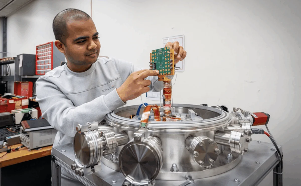
The centerpieces of the Department of Commerce announcement are substantial investments in both established technology giants and specialized quantum startups. IBM is slated to receive $1 billion to establish "Anderon," the nation’s first purpose-built 300mm quantum wafer foundry. This facility is expected to bridge the gap between experimental qubit production and the standardized manufacturing processes required for commercial-scale quantum systems. By utilizing 300mm silicon-on-insulator (SOI) wafers, IBM aims to leverage existing semiconductor fabrication techniques to increase qubit fidelity and yield.
GlobalFoundries, a major player in the contract manufacturing space, has been allocated $375 million to launch a dedicated domestic quantum foundry. This move signals a shift for the company toward high-value, specialized silicon-photonics and superconducting circuits that serve as the backbone for various quantum architectures.
The remaining funds are distributed among a cohort of companies focusing on diverse quantum modalities:

- Atom Computing and Infleqtion: Both companies received $100 million letters of intent to advance neutral-atom quantum computing. This approach uses lasers to trap and manipulate individual atoms, offering a promising path toward thousands of connected qubits.
- D-Wave: Allocated $100 million to further its work in both quantum annealing—currently used for optimization problems—and the development of universal gate-model systems.
- PsiQuantum: Granted $100 million to support the domestic manufacturing of critical photonics components, including optical switches and single-photon detectors, at its new facilities.
- Quantinuum and Rigetti: Each receiving up to $100 million, these companies focus on trapped-ion and superconducting architectures, respectively, emphasizing the government’s "all-of-the-above" strategy for quantum development.
- Diraq: A $38 million allocation supports the scaling of silicon-spin technology, which seeks to integrate quantum processors directly into existing CMOS manufacturing pipelines.
Accelerating the 2nm Transition and Advanced Packaging
While quantum computing represents the long-term horizon, the immediate semiconductor landscape is being reshaped by the move toward the 2nm process node. Mixel recently announced the availability of its MIPI C-PHY/D-PHY Combo Universal IP on TSMC’s N2P (2-nanometer) process. This development is critical for the next generation of mobile and automotive SoCs (System on Chips), providing the high-bandwidth interfaces necessary for advanced cameras and displays. The transition to N2P involves the adoption of Gate-All-Around (GAA) transistor architectures, which offer significant power and performance improvements over traditional FinFET designs.
In the realm of power electronics, Infineon has expanded its CoolGaN bidirectional switch family. These new devices are designed to reduce the physical footprint of power management systems on printed circuit boards (PCBs) by as much as 82%. By cutting component counts by half, these Gallium Nitride (GaN) switches allow for more efficient power delivery in data centers and electric vehicle (EV) charging infrastructure, where space and thermal management are at a premium.
AI-Driven Innovation in Extreme Environment Chip Design
The intersection of artificial intelligence and hardware design is yielding breakthroughs in specialized research. Fermilab is currently leading the AXESS initiative (Accelerating eXtreme Environment Specs-to-Silicon) in collaboration with Berkeley Lab and Siemens. The project aims to utilize AI to automate the design of custom integrated circuits capable of surviving extreme environments, such as the high-radiation zones of particle accelerators or the cryogenic temperatures required for deep-space exploration and quantum sensing.
Traditionally, designing chips for these "hardened" environments could take several years of iterative testing. The AXESS framework seeks to compress this timeline into a matter of weeks by using AI to predict material degradation and circuit failure under stress. This initiative is complemented by research at Rice University, where scientists have successfully developed large-scale films of chiral carbon nanotubes (CNTs). These CNT films demonstrate light-conversion properties that are two to three orders of magnitude more efficient than conventional materials, offering a new frontier for high-speed photonics and optical sensors.
Corporate Shifts: Digital Threads and Sovereign AI
In the private sector, major manufacturers are overhauling their internal workflows to keep pace with rapid innovation cycles. Quanta Computer, a leading electronics manufacturer for global brands, has integrated the Siemens Xcelerator software portfolio to create a "connected digital thread." This end-to-end integration of product lifecycle management (PLM) and manufacturing execution systems is intended to reduce the time for new product introductions by up to 25%.

Geopolitical pressures continue to drive the development of "Sovereign AI" infrastructure. Alibaba Cloud recently unveiled the Zhenwu M890, an AI accelerator chip developed by its T-Head semiconductor division. This launch is seen as a strategic move to reduce China’s reliance on high-end Nvidia GPUs, which have faced increasingly stringent export controls. Simultaneously, Nvidia is moving forward with its Vera CPUs, specifically designed to handle "agentic AI" workloads—autonomous systems capable of reasoning and executing complex tasks. Initial units have already been delivered to industry leaders such as OpenAI, SpaceXAI, and Anthropic.
Cybersecurity and the Rise of Agentic Threats
The 2026 cybersecurity landscape is increasingly defined by the exploitation of software vulnerabilities and the emergence of autonomous cyber agents. Verizon’s latest Data Breach Investigations Report (DBIR) identifies the exploitation of software flaws as the primary entry point for breaches, accounting for 31% of all successful attacks.
In response, the industry is moving toward a "detection-in-depth" framework. The Institute for AI Policy and Strategy (IAPS) has proposed a new defensive architecture that includes the use of "agent honeypots"—decoy environments designed to lure and identify autonomous AI attackers. Intel has also stepped up its efforts in this space, using AI to automate the detection of security gaps in hardware specifications before the chips even reach the fabrication stage. This proactive approach is essential as the complexity of modern chips makes manual verification increasingly prone to error.
Quantum Commercialization and Ecosystem Expansion
Beyond federal funding, the quantum industry is seeing significant private investment and strategic partnerships. Nord Quantique recently raised $30 million, bringing its valuation to approximately $1.4 billion as it pursues a roadmap toward fault-tolerant quantum computing by 2030.
Strategic collaborations are also bridging the gap between quantum hardware and industrial application. Quantinuum has partnered with Synopsys to integrate quantum algorithms into standard electronic design automation (EDA) tools. This partnership aims to allow engineers in life sciences and aerospace to use quantum-enhanced simulations for molecular modeling and structural analysis. Furthermore, PsiQuantum has solidified its global footprint by selecting Moreton Bay Central in Queensland as the site for its new Australian quantum facility, part of a broader international effort to build a utility-scale quantum computer.

Broader Implications and Industry Outlook
The convergence of multi-billion dollar government subsidies, the rise of AI-assisted design, and the push toward 2nm nodes indicates a semiconductor industry in a state of profound transformation. The U.S. government’s decision to take equity stakes in quantum companies marks a departure from traditional grant-based funding, suggesting a more hands-on approach to managing national technological assets.
As the industry prepares for upcoming events like the Electronic Components and Technology Conference (ECTC) and COMPUTEX Taipei, the focus remains on reliability and scalability. The automotive sector, in particular, is facing new challenges as chips become more central to vehicle safety and autonomy. Ensuring the long-term reliability of these components in harsh road environments is a priority, as evidenced by the growing emphasis on Design for Test (DFT) methodologies.
The next twelve to eighteen months will be a critical validation period for these investments. If the IBM and GlobalFoundries foundries can successfully standardize quantum chip production, and if AI can truly shorten custom silicon design cycles from years to weeks, the global technology landscape will shift permanently toward a more agile, decentralized, and computationally powerful era. The integration of quantum capabilities into mainstream EDA tools and the deployment of 2nm hardware will likely serve as the catalysts for the next wave of global economic growth, driven by the sheer scale of the "agentic era" and the arrival of utility-scale quantum systems.
