
The relentless march of semiconductor scaling continues to reshape the global packaging landscape, a movement fundamentally driven by the dictates of Moore’s Law and the escalating consumer demand for higher performance within increasingly compact form factors. Over the past two decades, transistor density has increased at an exponential rate, with leading-edge fabrication processes now achieving densities that exceed 100 million transistors per square millimeter. This rapid miniaturization has not occurred in a vacuum; rather, it has necessitated a parallel evolution in how these high-density integrated circuits (ICs) are housed, interconnected, and cooled. As the industry moves toward more complex systems-on-chip (SoC) and heterogeneous integration, the role of the package has shifted from a simple protective shell to a critical performance enabler.

Certain high-growth applications, specifically Radio Frequency (RF) components and Power Management Integrated Circuits (PMICs), have evolved alongside advanced-node components, creating a codependent ecosystem that operates under conditions of high frequency and increased current density. In these mixed-signal environments, high-performance devices generate significant localized heat, placing unprecedented thermal demands on adjacent legacy packages, such as the traditional wirebond MicroLeadFrame (MLF), also known as the Quad Flat No-lead (QFN) package. Consequently, modern MLF designs are currently confronting two critical existential challenges: the need for significantly improved electrical performance and the requirement for enhanced thermal dissipation. While traditional wirebond technology remains a staple of the industry due to its maturity, the emergence of Flip Chip MicroLeadFrame (fcMLF) technology represents a pivotal shift in addressing the bottlenecks of legacy packaging.
The Chronology of Packaging Evolution and the Flip-Chip Transition
The history of semiconductor packaging has been defined by the transition from through-hole mounting to surface-mount technology, and eventually to the sophisticated area-array and leadless packages used today. The MLF package, introduced widely in the late 1990s, became a dominant force in the industry due to its small footprint and excellent thermal properties compared to older plastic leaded chip carriers. However, for nearly twenty years, wirebonding—using thin gold or copper wires to connect the die to the leadframe—was the standard interconnect method.

As signal frequencies pushed into the multi-gigahertz range, the physical limitations of wirebonding became apparent. The length and loop height of bond wires introduce parasitic inductance and resistance that degrade signal integrity. In response, the industry began adopting flip-chip architectures, where the die is "flipped" and connected directly to the substrate or leadframe via conductive bumps. The development of fcMLF represents the maturation of this trend, combining the cost-effective and robust nature of the leadframe-based MLF with the high-performance interconnects of flip-chip technology. This transition has been accelerated by the rise of 5G communications, automotive electrification, and high-efficiency power delivery systems, all of which require the low-latency and high-thermal-efficiency characteristics that fcMLF provides.
Mitigating Electromagnetic Interference through Enhanced Electrical Performance
In high-frequency and high-power applications, Electromagnetic Interference (EMI) is a primary concern for system designers. Generated by a combination of factors, including impedance mismatch and parasitic elements, these electromagnetic emissions can result in logic errors, signal degradation, and catastrophic device malfunctions in sensitive peripheral nodes. To ensure global interoperability and safety, allowable levels of EMI are strictly outlined in international regulatory standards, such as those provided by the International Special Committee on Radio Interference (CISPR) and the Federal Communications Commission (FCC) Part 15 guidelines.

As integrated circuits achieve higher switching speeds, the density of components within compact systems increases, elevating EMI and signal integrity issues to the forefront of packaging design. Flip-chip solutions like fcMLF have emerged as critical enablers in this regard. A primary strategy for mitigating EMI involves ensuring a resonance-free system, which is achieved by identifying and matching impedance along the Input/Output (I/O) interconnect pathway. Package impedance is typically characterized using an electrical circuit model consisting of resistive, inductive, and capacitive elements (RLC).
Recent RLC simulations performed on various package types—including wirebond MLF, Flip Chip Chip Scale Package (fcCSP), and Wafer Level Chip Scale Package (WLCSP)—highlight the superior performance of fcMLF. At frequencies of 500 MHz and 1 GHz, fcMLF devices significantly outperform traditional wirebond MLF and fcCSP packages, nearly matching the impedance levels of WLCSP. Specifically, fcMLF simulated impedances were found to be 2.3 times lower than those of wirebond MLF devices. This reduction in impedance provides designers with significantly greater flexibility in Printed Circuit Board (PCB) layouts, allowing for more efficient placement of peripheral components required for signal level matching. Furthermore, in PMIC applications, successful impedance matching reduces potential voltage drops or spikes, which is essential for maintaining the stability of the power delivery network (PDN).

Addressing Parasitic Inductance and Signal Integrity
Beyond EMI, parasitic inductance remains a critical factor influencing signal fidelity. Parasitics arise from the inductive elements within a package—namely bond wires, vias, and traces—which can distort signal waveforms during fast switching events. At high frequencies, even minute inductive values can lead to substantial voltage spikes, contributing to overshoot and undershoot. This phenomenon results in signal ringing, which degrades the overall reliability of the data transmission.
Traditional wirebond packages are particularly susceptible to parasitic inductance because of their relatively long and variable interconnect paths. In contrast, fcMLF utilizes copper pillar bumping for die-to-package interconnects. This method enables much shorter electrical signal paths, directly reducing the interconnect length and, consequently, the parasitic inductance. Simulation data indicates that fcMLF achieves an inductance value as low as 0.4nH, outperforming both wirebond MLF and fcCSP. By optimizing both inductance and impedance, fcMLF supports reliable operation in the high-speed, high-power environments typical of modern RF and power management applications.

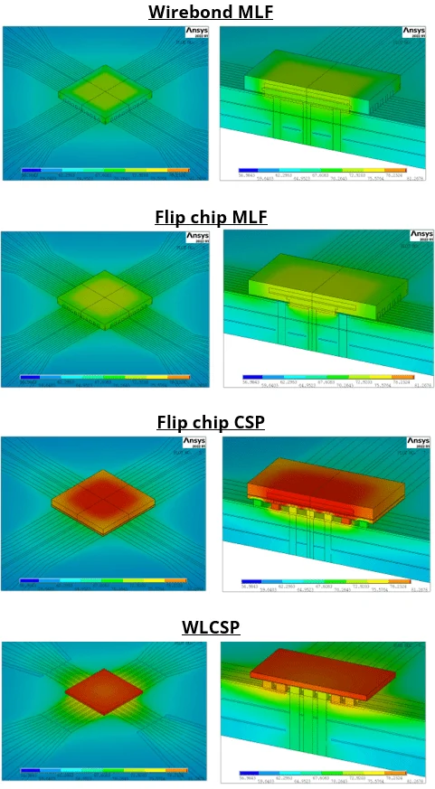
Thermal Dissipation: Solving the High-Power Density Crisis
As die-level power densities continue to rise, the ability of a package to dissipate heat effectively has become a bottleneck for system performance. The trend toward miniaturization further complicates this issue by concentrating thermal energy into smaller volumes. Effective thermal management is not merely a matter of performance; it is a requirement for long-term device reliability, as excessive heat accelerates semiconductor aging and failure mechanisms.
The leadframe-based structure of fcMLF is uniquely suited to meet these challenges. Unlike traditional wirebond MLF configurations, fcMLF allows for thermal enhancement on both the top and bottom of the die. In a typical fcMLF design, an exposed die attach pad is utilized, supporting multiple die-level thermal vias attached directly to the pad. This architecture enables highly efficient thermal dissipation into the PCB through ground plane interconnects.

Thermal modeling comparing various package types reveals that fcMLF closely matches the junction-to-ambient thermal resistance ($Thetaja$) of wirebond MLF (36.1 vs. 33.6 °C/W), while significantly outperforming fcCSP and WLCSP, which often exceed 50 °C/W. More impressively, the junction-to-board thermal resistance ($Thetajb$) for fcMLF is approximately 2 to 5 times lower than that of competing designs. This drastic reduction in $Theta_jb$ means that under equivalent power loads, the fcMLF package will experience a much smaller temperature increase, ensuring that the silicon remains within its optimal operating temperature range even in high-power density applications like DC/DC converters.
Dimensional Innovation and Package Characteristics
The demand for thinner and smaller electronic devices has forced packaging engineers to rethink the physical architecture of the MLF. In a traditional wirebond MLF, the package footprint and height are constrained by the need to place bond pads along the periphery and the requirement for a mold cap thick enough to enclose the wire loops. Typically, a distance of 100 $mu$m or more is required between the die top and the mold cap to accommodate these wires.

By replacing wire bonds with copper pillars, fcMLF allows interconnect pads to be moved directly beneath the die. This shift enables a significant reduction in both the package footprint and height. With a nominal copper pillar bump height of 80 $mu$m and the use of thinned silicon dies, fcMLF solutions can achieve a total package thickness of less than 350 $mu$m. This profile is significantly lower than the 350–400 $mu$m common in traditional wirebond MLF packages, making fcMLF an ideal choice for space-constrained mobile and wearable applications.
Quality Assurance: The Wettable Flank Advantage
One of the historical challenges with leadless packages like the MLF has been the difficulty of inspecting solder joints after the package is mounted on a PCB. Traditional designs often require X-ray inspection to verify the integrity of the hidden solder connections, a process that is both time-consuming and expensive. To address this, fcMLF incorporates a "wettable flank" step-cut design.

This feature exposes a portion of the leadframe sidewall, allowing solder to "wick" up the side of the package during the reflow process. This creates a visible solder fillet that can be inspected using Automated Optical Inspection (AOI) equipment. The ability to use AOI rather than X-ray is a significant advantage for high-volume manufacturing, as it reduces inspection costs and improves throughput. Furthermore, it eliminates the need for the specific component spacing often required to facilitate X-ray penetration, allowing for denser PCB layouts.
Manufacturing Synergy and Economic Implications
The semiconductor industry is highly sensitive to capital expenditure and manufacturing complexity. One of the most compelling aspects of fcMLF technology is its compatibility with existing, mature MLF manufacturing infrastructure. MLF technology is a well-established process with a robust ecosystem of tooling, materials, and process controls already in place for automotive and consumer electronics.

The fcMLF manufacturing flow utilizes much of this established infrastructure, adding only the die flip-chip attachment and reflow processes. By using the same copper leadframe materials as traditional MLF, manufacturers can maintain consistent supply chains and reduce the cycle time for new product introductions. This manufacturing synergy not only lowers the cost of assembly but also accelerates time-to-market for chip designers. For companies looking to upgrade their product performance without a total overhaul of their assembly lines, fcMLF offers a seamless transition path.
Broader Impact and Future Outlook
The introduction and refinement of fcMLF technology have broad implications for the semiconductor industry. As automotive systems transition toward autonomous driving and electrification, the need for robust, thermally efficient, and EMI-resistant packaging will only grow. In the consumer space, the integration of 5G and AI-capable processors into smaller devices will require the high-end capabilities that fcMLF delivers at a cost-effective scale.

Industry analysts suggest that the move toward flip-chip leadframe solutions is a necessary step in the bridging of the gap between low-cost legacy packaging and high-cost advanced substrates. By delivering high-end electrical and thermal performance in a compact, leadframe-based format, fcMLF stands as a robust solution that balances innovation with practicality. As power densities continue to climb and signal speeds reach new thresholds, the strategic adoption of fcMLF is expected to become a standard practice for designers of PMICs, RF devices, and high-performance power converters worldwide. This evolution ensures that the packaging industry can continue to support the ambitious goals of the broader semiconductor roadmap for years to come.
