
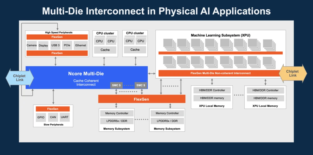

The global semiconductor industry is currently navigating a fundamental shift in architectural design, moving away from massive monolithic Systems-on-Chip (SoCs) toward sophisticated, multi-die chiplet-based systems. This transition is not merely a manufacturing preference driven by yield optimization and cost; it is a technical necessity forced by the rapid evolution of Physical AI. Unlike traditional cloud-based AI, which often relies on batch processing and data center-scale infrastructure, Physical AI involves systems that must perceive, reason, and act in real-time environments. From autonomous vehicles navigating complex urban intersections to industrial robots performing precision manufacturing, these systems require a continuous, high-volume data flow between heterogeneous compute engines that monolithic silicon can no longer support efficiently.
The Architectural Mismatch
For the past two decades, die-to-die communication has been dominated by coherent interconnect protocols. These protocols were architected to support processor-centric systems where the primary goal was maintaining memory consistency across multiple CPU cores. In these environments, communication is characterized by frequent, small, cache-line-sized transactions. While highly effective for general-purpose computing, these protocols are increasingly viewed as a bottleneck for the data-heavy workloads of modern AI accelerators.
In a Physical AI system, the traffic patterns are fundamentally different. A modern automotive compute platform, for instance, must simultaneously process LiDAR point clouds, high-resolution video streams for computer vision, sensor fusion algorithms, and real-time path planning. These tasks generate massive, continuous streams of tensors, feature maps, and intermediate inference results. When these streams are forced through traditional coherent protocols, the overhead—such as cache-coherency probes, snoop requests, and state-machine transitions—consumes an disproportionate amount of available bandwidth. Consequently, the industry is witnessing a "protocol tax" where the actual data payload accounts for only a fraction of the transmitted bandwidth, limiting the scalability of next-generation AI platforms.
Chronology of the Interconnect Evolution
The industry’s path to the current bottleneck can be traced through several distinct phases of evolution:
- The Era of Monolithic Integration (2000–2015): The industry focused on cramming more transistors onto a single piece of silicon. Interconnects were internal, proprietary, and highly optimized for the specific NoC (Network-on-Chip) topology of that chip.
- The Rise of Heterogeneous Computing (2015–2020): As power density limits and reticle size constraints emerged, companies began offloading tasks to specialized accelerators (GPUs, TPUs, NPUs). Interconnects like AXI were extended to bridge these blocks, but these remained largely control-oriented.
- The Chiplet Paradigm (2020–Present): With the arrival of advanced packaging (such as 2.5D and 3D stacking), engineers began partitioning SoCs into chiplets. However, the communication protocols used to bridge these chiplets—such as CXL or UCIe in their current implementations—have struggled to keep pace with the sheer volume of accelerator-to-accelerator traffic required by high-end AI models.
Supporting Data and Efficiency Analysis
The inefficiency of current standards is quantifiable. Most coherent protocols divide communication into 64-byte cache-line transactions. Each transaction requires substantial metadata. When an AI accelerator transmits a 10-megabyte tensor, it must fragment this data into approximately 163,840 individual transactions. Each of these transactions carries its own header, error correction, and coherence signaling.
As AI bandwidth requirements scale into the terabytes per second, this metadata-to-payload ratio becomes unsustainable. Industry benchmarks indicate that in dataflow-heavy workloads, protocol overhead can consume between 20% and 40% of the total die-to-die bandwidth. By moving to a native, packetized NoC approach—where the NoC effectively spans the physical gap between dies—this overhead can be reduced by more than 50%. By treating the remote chiplet as just another node in the existing internal network, engineers eliminate the need for costly, high-latency conversion steps at every die boundary.
The Rise of Physical AI Requirements
The demands of Physical AI in automotive and robotics sectors are rigorous. Unlike consumer electronics, these systems are safety-critical. They require:

- Determinism: Data must arrive at predictable intervals to ensure real-time response times.
- Low Latency: In a high-speed vehicle, the time taken for a sensor to trigger an inference result must be minimized to the microsecond level.
- Thermal Constraints: As power envelopes are limited, every milliwatt spent on protocol overhead is a milliwatt that cannot be used for compute, directly impacting the system’s performance ceiling.
Leading semiconductor architects and industry analysts have noted that the "transaction layer" approach—where NoC packets are converted into AXI transactions to cross a boundary, then reassembled—is becoming the primary source of latency in modern multi-die designs. Each conversion step necessitates buffering, which not only increases latency but also increases the silicon footprint of the interface logic.
Towards an Invariant NoC Interface
To solve this, the industry is moving toward a standard for "invariant" die-to-die NoC interfaces. The goal is to provide a stable architectural bridge that separates the internal implementation of a chiplet from the transport layer. This allows a design team to update their internal NoC protocol to support new features—such as improved Quality of Service (QoS), enhanced security, or advanced power management—without needing to redesign the die-to-die physical interface.
An invariant interface provides:
- Protocol Agnosticism: It treats data as a stream of packets, regardless of whether that data originated from a CPU cache request or a raw tensor stream.
- Virtual Channel Support: It enables the multiplexing of multiple traffic types, allowing high-priority safety data to bypass low-priority background tasks.
- Scalability: The interface can be widened or narrowed depending on the bandwidth needs of the specific chiplet pairing without altering the underlying logic.
Broader Impact and Industry Implications
The transition to a direct NoC-to-NoC transport architecture is poised to reshape the supply chain. For chiplet designers, this approach offers a level of modularity that was previously unattainable. Companies can now mix and match chiplets from different process nodes—for example, combining a high-performance 3nm compute chiplet with a more mature 7nm I/O chiplet—without worrying about protocol incompatibility at the boundary.
This modularity is particularly vital for the automotive industry, which operates on long product lifecycles. If an automaker wants to update its AI inference chiplet for a new model year, a standardized, invariant NoC interface allows for a "plug-and-play" upgrade path. The vehicle’s central compute backbone remains stable, while the performance-critical AI engines can evolve at the speed of software innovation.
Furthermore, the shift has profound implications for functional safety. By simplifying the interface logic and reducing the number of gates required for transaction conversion, the potential for hardware bugs and logical errors is reduced. In safety-critical systems, simplicity is often the most effective form of reliability.
Conclusion
As Physical AI continues to integrate into the fabric of daily life—from the cars we drive to the factories that power our economy—the bottleneck of on-chip and off-chip communication will remain a central challenge. The move away from rigid, coherent-centric protocols toward flexible, native NoC-to-NoC transport represents a maturation of the chiplet ecosystem. By prioritizing dataflow efficiency over legacy memory-consistency models, the semiconductor industry is aligning its communication architectures with the realities of modern AI workloads. This shift not only promises higher throughput and lower energy consumption but also provides the long-term architectural stability required for the next decade of intelligent, real-world computing. The future of AI performance lies not just in the speed of the transistors, but in the efficiency and agility of the networks that connect them across the die boundary.
