
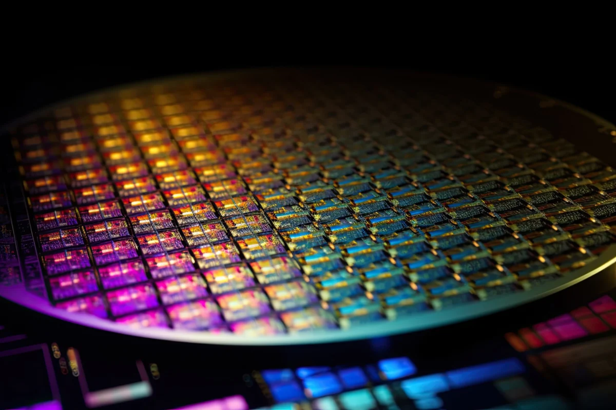

The global semiconductor industry stands at a critical juncture where traditional scaling methods are meeting the physical limits of materials and the logistical constraints of diagnostic testing. Recent collaborative research from international institutions has introduced three transformative developments that address these challenges: a tandem neural network for near-instantaneous material characterization, the discovery of ferroelectric properties in ultra-thin titanium dioxide, and the invention of bidirectional pixels capable of simultaneous light emission and analysis. These innovations collectively represent a shift toward more efficient, intelligent, and compact electronic systems.
Accelerating Semiconductor Characterization via Tandem Neural Networks
The process of developing and manufacturing semiconductors involves a rigorous phase of material characterization, where physical parameters must be extracted from electrical measurements. Traditionally, this process has relied on device-simulation-based methods, such as Technology Computer-Aided Design (TCAD). While accurate, TCAD requires hundreds of iterative calculations to solve "inverse problems"—the process of working backward from observed electrical behavior to determine the underlying physical properties of the material. This workflow can take anywhere from several hours to several days for a single dataset.
To circumvent this bottleneck, researchers from the Institute of Science Tokyo, Yokohama City University, and National Sun Yat-sen University have developed a tandem neural network (TNN) architecture. This system is specifically designed to solve the "multivaluedness" problem, where different sets of physical parameters might result in the same observed electrical output, often leading conventional machine learning models to provide mathematically correct but physically impossible solutions.
Technical Architecture and Performance Data
The TNN operates through two interconnected models. The first is an inverse model that estimates material properties based on transistor measurements. The second is a pre-trained forward network that takes those estimates and reconstructs the original transistor characteristics. By comparing the reconstructed output with the initial input, the system creates a feedback loop that ensures the predicted physical parameters are consistent with the laws of physics.
In experimental trials, the TNN was trained using 1,000 datasets derived from amorphous indium–gallium–zinc oxide (a-IGZO) transistors. The model focused on six critical physical parameters:
- Defect densities within the material.
- Trap-state characteristics at the interfaces.
- Electron mobility.
- Characteristic energy of the sub-gap states.
- Flat-band voltage.
- Doping concentrations.
The results demonstrated that the TNN could infer all six parameters from a single current-voltage (I-V) curve in less than one millisecond. According to Associate Professor Keisuke Ide of the Institute of Science Tokyo, this represents a speedup of over six orders of magnitude compared to iterative simulation methods. Furthermore, when tested against real-world transistors fabricated in a laboratory setting, the TNN accurately reproduced measured behaviors without requiring manual optimization or post-processing adjustments.
Implications for High-Volume Manufacturing
The ability to perform real-time characterization has profound implications for semiconductor fabrication. In a high-volume manufacturing environment, the TNN could be integrated into in-line metrology tools, allowing for instantaneous quality control. If a batch of wafers deviates from the target specifications, engineers could identify the exact physical parameter responsible for the drift within seconds, rather than waiting days for simulation results. This speed is expected to significantly reduce waste and accelerate the development cycle for new material compositions.
The Emergence of Atomic-Scale Ferroelectricity in Titanium Dioxide
While diagnostic speed is increasing, the search for new materials to sustain Moore’s Law continues. A research consortium involving the University of California Berkeley, Lawrence Berkeley National Laboratory, and SLAC National Accelerator Laboratory has reported a breakthrough in the behavior of titanium dioxide (TiO₂). Traditionally utilized as a dielectric (insulating) material in capacitors and gate oxides, TiO₂ has been found to exhibit ferroelectric properties when scaled down to the atomic level.
Ferroelectricity is a property where a material maintains a spontaneous electric polarization that can be reversed by an external electric field. This characteristic is highly sought after for the development of non-volatile memory and low-power logic devices, such as Ferroelectric Field-Effect Transistors (FeFETs).
Discovery and Substrate Versatility
The research team discovered that when the thickness of TiO₂ films is reduced below 3 nanometers (nm), the material undergoes a phase transition into a ferroelectric state. Professor Sayeef Salahuddin of UC Berkeley noted that this behavior remains stable even at thicknesses of approximately 1 nm, which corresponds to roughly two unit-cells of the material.
One of the most significant aspects of this discovery is the material’s stability across diverse substrates. The ferroelectric phase was maintained on:
- Crystalline silicon (the industry standard for chips).
- Amorphous carbon films.
- Various metallic substrates.
This versatility suggests that TiO₂ could be integrated into existing CMOS (Complementary Metal-Oxide-Semiconductor) workflows without the compatibility issues that plague other ferroelectric materials like hafnium oxide or perovskites.
Manufacturing and Integration Potential
The TiO₂ films were grown using Atomic Layer Deposition (ALD), a standard technique in modern semiconductor fabrication that allows for precise control over thickness at the atomic level. The process was conducted at temperatures below 400°C. This "thermal budget" is critical for Back-End-of-Line (BEOL) integration, where new layers are deposited on top of existing transistors. Temperatures exceeding 400°C often damage the underlying copper interconnects and sensitive transistor structures.
By enabling ferroelectricity at low temperatures and ultra-thin scales, TiO₂ opens the door for 3D integrated electronics. These could include high-density memory stacked directly on top of logic layers, significantly reducing the physical distance data must travel and thereby lowering power consumption and heat generation.
Bidirectional Fourier Pixels: Merging Sensing and Display
The third major innovation comes from the field of photonics, where researchers at ETH Zurich have reimagined the fundamental unit of digital imaging: the pixel. Traditional pixels are unidirectional; they either emit light (as in an OLED display) or capture it (as in a CMOS image sensor). The ETH Zurich team has developed "bidirectional pixels" that can perform both functions simultaneously through a single structure.
The Principle of Fourier Optics
These new "Fourier pixels" utilize wave-shaped, nano-sculpted surfaces. To emit or steer light, the pixel converts incoming electrical or optical energy into a surface wave that propagates across the chip. At a specific junction, this surface wave is scattered back out as a light wave. By precisely engineering the surface patterns, the researchers can control the interference of these waves to create specific images or light patterns.
Conversely, the same pixel can analyze incoming light. By applying the principles of Fourier analysis—a mathematical method used to decompose signals into their constituent frequencies—the pixel can determine:
- Amplitude: The intensity of the light.
- Phase: The position of the light wave in its oscillation cycle.
- Polarization: The orientation of the light wave’s vibrations.
Sander Vonk, a postdoctoral researcher at ETH Zurich, explained that the ability to capture phase and polarization is particularly significant. While standard cameras only record intensity (amplitude), capturing phase allows for the reconstruction of 3D information, potentially enabling holographic imaging and advanced depth sensing without the need for bulky external lenses.
Chronology of Development and Future Applications
The development of the Fourier pixel follows years of research into metasurfaces—materials engineered to have properties not found in nature. The ETH team’s successful demonstration of a single bidirectional pixel marks the transition from theoretical physics to functional hardware. The next phase of the project involves scaling these individual pixels into a massive matrix.
The implications for consumer and industrial technology are vast. Potential applications include:
- Invisible Cameras: Displays that can "see" through themselves, eliminating the need for "notches" or "punch-holes" in smartphones and laptops.
- Advanced Augmented Reality (AR): Lightweight glasses that can project images onto the eye while simultaneously tracking eye movement and mapping the environment using the same pixels.
- Secure Communications: Optical chips that can transmit and receive encrypted data using polarization states that are difficult to intercept or spoof.
Synthesizing the Future of Electronics
The convergence of these three technologies—AI-driven diagnostics, atomic-scale ferroelectrics, and bidirectional photonics—points toward a future where electronic devices are not only smaller and faster but also more integrated.
The timeline for these technologies suggests a phased rollout. The Tandem Neural Network approach is likely the closest to industrial adoption, as it requires no new hardware, only the implementation of new software protocols in existing characterization labs. The ferroelectric TiO₂ thin films could follow within the next three to five years as manufacturers look for ways to extend the life of silicon-based architectures. The bidirectional pixels represent a longer-term shift in how we conceive of displays and sensors, potentially reaching the market in the late 2020s or early 2030s.
By reducing the time required for material analysis from days to milliseconds, enabling non-volatile memory at the 1nm scale, and merging the functions of cameras and screens, these research breakthroughs provide a roadmap for the next decade of innovation. They address the dual needs of the modern world: the demand for higher performance and the urgent necessity for more energy-efficient, sustainable computing.
