
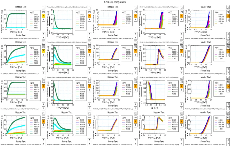

The quantum computing landscape is currently undergoing a structural evolution, transitioning from isolated, experimental research setups to large-scale, integrated systems. As the industry moves toward high-qubit-count processors, the challenge of control and readout electronics has become the primary bottleneck for scalability. With the quantum market projected to grow at a Compound Annual Growth Rate (CAGR) of 41.8% between 2025 and 2030, according to industry analysts at MarketsandMarkets, the demand for reliable, cryogenically compatible semiconductor hardware has never been higher. At the heart of this challenge lies the need for accurate device modeling, as traditional semiconductor models designed for room-temperature operations fail to capture the complex, non-linear physics occurring just a few degrees above absolute zero.
The Physics of the Cryogenic Frontier
In standard silicon-based electronics, devices are engineered to operate at approximately 300K (27°C). However, quantum processors, particularly those based on superconducting qubits, must operate in dilution refrigerators at temperatures as low as 4K (-269°C) or even lower, in the millikelvin range. When semiconductor devices—the very transistors that make up the control and readout circuitry—are cooled to these temperatures, their fundamental behavior shifts dramatically.

Key parameters such as threshold voltage, carrier transport, leakage current, and transconductance undergo significant alterations. Below 10K, effects that are typically negligible at room temperature become dominant. Dopant freeze-out, a phenomenon where charge carriers lose the thermal energy required to move through the silicon lattice, alters the conductivity of the material. Furthermore, changes in carrier statistics and the fundamental band structure of the semiconductor necessitate a complete rethinking of how we model these circuits. Without precise models, engineers face a "black box" scenario, unable to reliably simulate the performance of low-noise amplifiers or control logic, which leads to massive inefficiencies in the design cycle.
A Chronology of the Modeling Bottleneck
The history of semiconductor modeling has long relied on physics-based compact models, such as the industry-standard BSIM (Berkeley Short-channel IGFET Model). For decades, these models have been the gold standard for integrated circuit design. However, the roadmap of quantum development has outpaced the development of standard models for extreme low temperatures.
- 2015–2020: Quantum research was largely characterized by "home-grown" electronics. Engineers manually tuned models to fit experimental data at 4K, a process that was often non-transferable and lacked the rigor required for commercial-grade chip manufacturing.
- 2021–2023: As the industry shifted toward cloud-based quantum deployments, the necessity for standardized cryogenic libraries became clear. Researchers struggled with the "standardization gap," as there was no consensus on how to incorporate sub-10K physics into existing BSIM frameworks.
- 2024–2026: The emergence of Machine Learning (ML) optimizers began to change the trajectory. By moving away from manual, iterative parameter tuning—which often trapped engineers in local minima during the extraction process—the industry began adopting automated, derivative-free optimization techniques.
The Hybrid ANN Approach: A Technical Synthesis
The current industry standard, spearheaded by solutions such as Keysight’s IC-CAP platform, involves a sophisticated hybrid approach that merges the reliability of physics-based models with the predictive power of Artificial Neural Networks (ANNs).
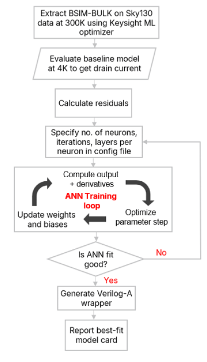
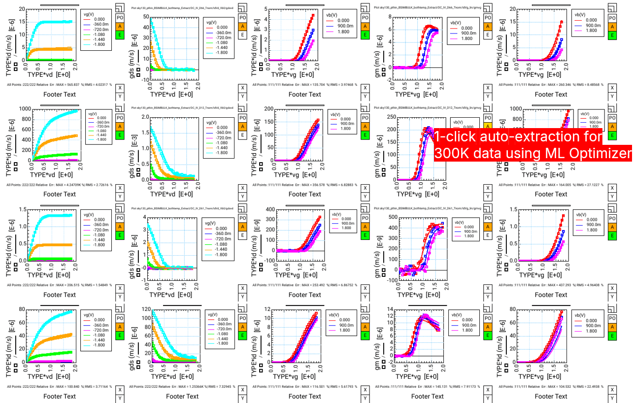
The methodology begins with the extraction of a high-quality baseline model at room temperature (300K) using BSIM-BULK. By utilizing an ML-based optimizer, engineers can simultaneously extract over 80 critical parameters in a single, efficient step. This establishes a robust "physics-based reference." Once this baseline is established, the model is tested against 4K measurement data.
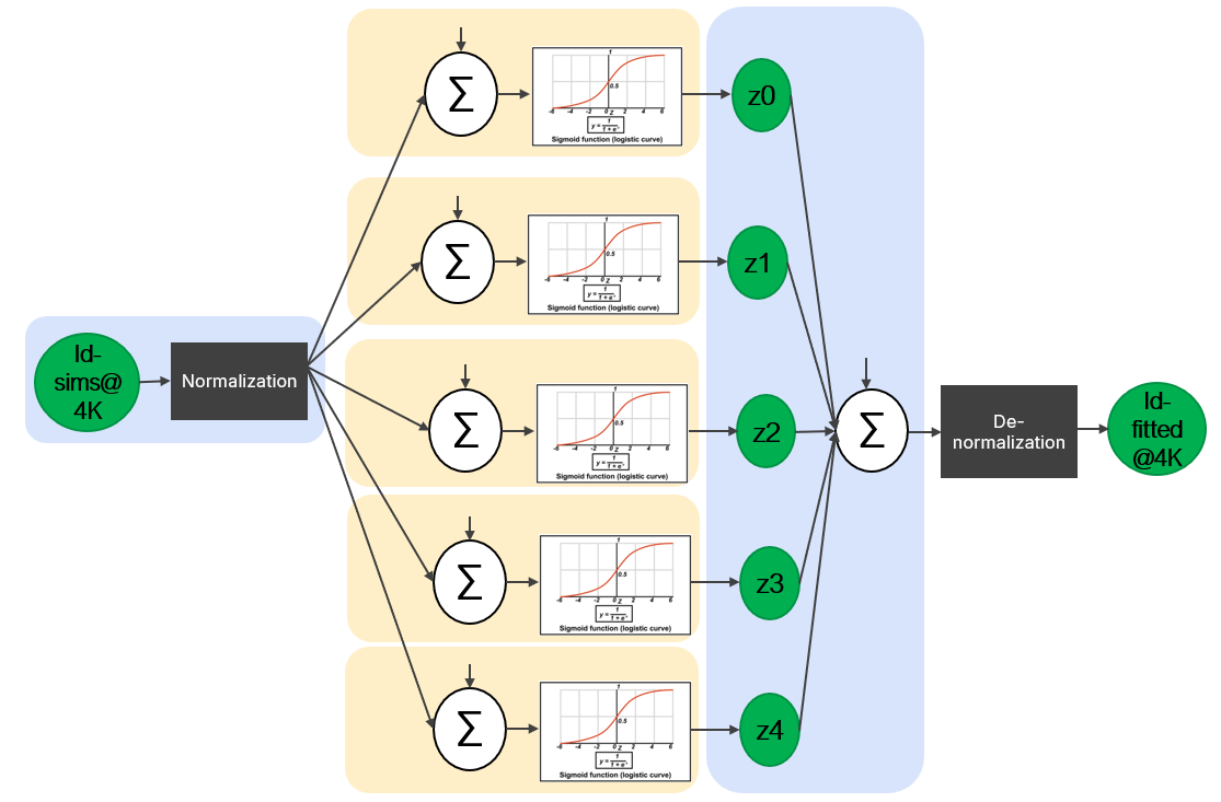
Because BSIM-BULK lacks the specific equations to account for cryogenic physical phenomena, the model produces "residuals"—the difference between the simulation and the actual measured data. Instead of attempting to rewrite complex physics equations from scratch, engineers now employ a hybrid ANN. This neural network acts as an intelligent correction layer, specifically learning the residual behavior of the device at 4K. By training a forward-propagation ANN with two hidden layers, the system can map the bias and geometry-dependent interactions that physics models miss. The result is a highly accurate, Verilog-A compatible model that can be implemented in standard circuit simulation environments.
Implications for Quantum Scalability
The implications of this breakthrough are significant for the broader semiconductor and quantum industries. By reducing the time required to develop cryogenic models from months of manual labor to mere minutes of automated computation, companies can accelerate the design cycle for control electronics.
- System-Level Optimization: With accurate models in hand, designers can now perform system-level simulations that include the quantum processor and its associated control hardware simultaneously. This reduces the risk of thermal runaway or signal degradation at the chip interface.
- Cost Reduction: The ability to simulate before fabrication is the bedrock of the semiconductor industry. Providing this capability to the quantum sector lowers the cost of entry for startups and accelerates R&D for large enterprises.
- Cross-Platform Portability: Because the hybrid ANN equations can be converted into Verilog-A, these models are portable across different electronic design automation (EDA) tools, allowing for a more cohesive design ecosystem.
Industry Perspective and Future Outlook
While companies like Keysight are leading the charge in providing these modeling tools, the broader industry is reacting with a renewed focus on cryogenic CMOS (cryo-CMOS). Analysts note that the integration of control electronics onto the same wafer as the quantum processor—or onto a closely coupled cryo-electronics wafer—is the only viable path to scaling systems beyond the current limitations of room-temperature cabling.
"The challenge is no longer just about the qubits," noted an industry consultant familiar with the technology. "It is about the entire signal chain. If we cannot model the silicon that talks to the quantum processor at 4K, we cannot hope to scale to thousands or millions of qubits."
The integration of AI into device modeling is not merely a convenience; it is a fundamental requirement for the next phase of quantum development. By leveraging the combined strengths of deterministic physics and probabilistic machine learning, the industry has found a way to bridge the gap between our current silicon capabilities and the requirements of the quantum era.
As we look toward 2030, the ability to rapidly characterize and model semiconductor behavior at cryogenic temperatures will likely become a competitive differentiator. Firms that adopt these AI-driven workflows will be positioned to design more efficient, reliable, and scalable quantum systems, effectively turning the "cryogenic challenge" into a manageable engineering task. The integration of these models into standard design flows signifies the maturation of quantum computing from a scientific endeavor into a robust, industrial-scale technology.
