

The semiconductor industry is currently undergoing a fundamental shift as artificial intelligence migrates from massive, centralized data centers to the diverse and resource-constrained landscape of edge computing. This transition, moving from large language models (LLMs) hosted in the cloud to small language models (SLMs) running locally on devices, represents one of the most significant engineering challenges of the decade. As companies seek to deploy sophisticated AI capabilities in everything from automotive sensors to consumer electronics, the demand for specialized Neural Processing Units (NPUs) has surged. However, the industry faces a persistent paradox: the more a hardware architecture is optimized for a specific task to gain efficiency, the more it risks becoming obsolete as AI algorithms evolve.
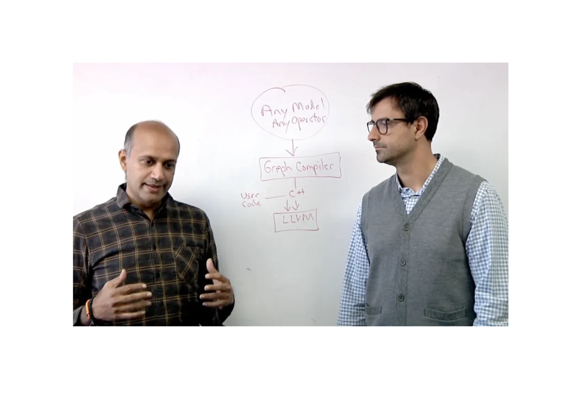
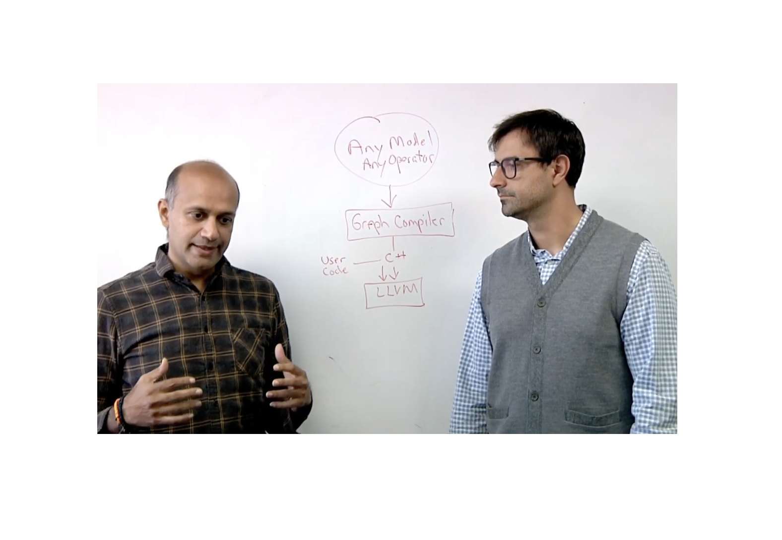
In a recent technical discussion led by Ed Sperling, editor-in-chief of Semiconductor Engineering, Daniel Firu, Chief Product Officer and co-founder of Quadric, and Ravi Chakaravarthy, Vice President of Software at Quadric, explored the intricate balance required to build next-generation NPUs. The dialogue highlighted that the journey to the edge is not merely a matter of shrinking existing algorithms but requires a total rethink of the hardware-software interface. To succeed, modern NPUs must deliver the high-performance throughput of a dedicated accelerator while maintaining the programmable flexibility of a general-purpose processor.
The Evolution of Edge AI Architecture
The chronology of AI hardware development has moved through three distinct phases. In the early 2010s, AI was primarily the domain of General-Purpose Graphic Processing Units (GPGPUs), which provided the parallel processing power necessary for deep learning but consumed massive amounts of energy. By the mid-2010s, the industry saw a move toward Application-Specific Integrated Circuits (ASICs) and fixed-function NPUs. These devices were incredibly efficient at performing the matrix multiplications required by convolutional neural networks (CNNs), but they were "brittle"—any change in the underlying mathematical model often rendered the hardware inefficient or unusable.
Today, the industry has entered a third phase characterized by the need for domain-specific flexibility. The rapid rise of Transformer-based architectures and the emergence of SLMs have proven that AI models are moving targets. An NPU designed in 2022 specifically for CNNs might struggle with the attention mechanisms required by modern Generative AI. This has forced architects to reconsider the "hard-wired" approach. The current objective is to create a unified compute fabric that can handle both the predictable, heavy-lifting math of neural networks and the unpredictable, "scalar" code that often surrounds these models in real-world applications.
The Complexity of Moving from Cloud to Edge
Moving AI to the edge involves navigating a minefield of constraints that do not exist in the cloud. In a data center, power is a managed utility and cooling is a solved engineering problem. At the edge, engineers are often limited by a power envelope of less than 5 Watts, limited thermal dissipation capabilities, and a strict cost-per-die requirement.
Furthermore, the "Small Language Model" (SLM) is a relative term. While an LLM might have 175 billion parameters, an SLM designed for the edge might still have 1 billion to 7 billion parameters. Running such a model on a device with limited LPDDR memory requires aggressive optimization techniques. Daniel Firu noted that the constraints vary wildly between market segments. For instance, an NPU in an industrial IoT gateway might prioritize 24/7 reliability and low latency for anomaly detection, while an NPU in a premium smartphone must prioritize peak performance for photography and real-time translation while maximizing battery life.
Data supporting this shift suggests that the edge AI market is expected to grow at a compound annual growth rate (CAGR) of over 20% through 2030. This growth is driven by the realization that cloud-based AI is often too slow (latency), too expensive (bandwidth costs), and too invasive (privacy concerns) for many critical applications.
Balancing Hardware Specialization and Software Programmability
One of the central themes discussed by the Quadric executives was the danger of "over-specialization." In the pursuit of high TOPS (Tera Operations Per Second) per Watt, many designers strip away the ability of the processor to handle non-AI tasks. However, a real-world AI pipeline is rarely just a neural network; it involves pre-processing (scaling, cropping, color conversion) and post-processing (non-maximum suppression, decision logic).
Ravi Chakaravarthy emphasized that the software stack is the most critical component in maintaining flexibility. Historically, NPUs required developers to write code in low-level, proprietary languages or use complex toolchains that were difficult to debug. This created a "wall" between the data scientist developing the model and the embedded engineer trying to run it.
To break down this wall, the industry is increasingly looking toward a "software-first" design philosophy. This involves building hardware that can be targeted by standard C++ and high-level machine learning frameworks. By ensuring the NPU can handle both the heavy matrix math and the "messy" control-flow code, developers can avoid the latency penalties associated with moving data back and forth between a dedicated NPU and a companion CPU.
The Role of Open Source and Unified Toolchains
The discussion also touched upon the strategic use of open-source ecosystems. Rather than reinventing the wheel, modern NPU providers are leveraging frameworks like Apache TVM, MLIR (Multi-Level Intermediate Representation), and Glow. These tools allow for a more standardized way of compiling models from high-level frameworks like PyTorch and TensorFlow down to the specific machine code of the NPU.
Chakaravarthy noted that adding value in this environment means providing the "last mile" of optimization. While open-source tools provide the foundation, a proprietary compiler can provide the specific hardware-aware optimizations—such as memory banking, register allocation, and pipeline scheduling—that allow a chip to reach its theoretical performance limits. This hybrid approach allows semiconductor companies to benefit from the rapid community-driven innovations in AI while protecting their unique hardware advantages.
Market Segment Variability and Deployment Realities
The requirements for customization change significantly depending on the end-use case. The panel identified several key segments:

- Automotive: Here, safety and predictability are paramount. NPUs must be ISO 26262 compliant. The flexibility is needed not just for new AI models, but to handle different types of sensor fusion (LiDAR, Radar, and Vision) simultaneously.
- Consumer Electronics: In devices like smart glasses or wearables, the primary constraint is the "thermal ceiling." If a chip gets too hot, it must throttle performance. Customizing an NPU for these devices involves optimizing for "leakage" power and ensuring the software can dynamically scale workloads.
- Industrial and Medical: These segments require long lifecycles. An NPU deployed today in a medical imaging device might need to be supported for 10 to 15 years. This necessitates a programmable architecture that can be updated via firmware as new diagnostic AI models are FDA-approved.
Technical Analysis: The Efficiency-Flexibility Trade-off
The core of the NPU design challenge lies in the "area efficiency" of the silicon. A fixed-function multiplier is much smaller and more power-efficient than a programmable logic unit. However, if that fixed-function logic cannot support a new type of activation function or a different bit-precision (moving from INT8 to FP8 or binary weights), that silicon area becomes "dead weight."
Current research suggests that the most successful NPU architectures are moving toward a heterogeneous "tiled" approach. In this model, the chip consists of a grid of processing elements. Some tiles are optimized for massive parallel math, while others are more general-purpose in nature. A sophisticated compiler then maps the AI graph across these tiles, ensuring that data movement is minimized. This reduces the energy-intensive "memory wall" problem, where the power spent moving data from memory to the processor exceeds the power spent on the actual computation.
Official Perspectives and Future Implications
The insights from Firu and Chakaravarthy suggest that the future of the NPU market will not be won by the company with the highest "peak TOPS" on a datasheet, but by the company that offers the most seamless "time to market." If a developer cannot port a model from a workstation to an edge device in a matter of days, the hardware is a failure.
The broader implication for the semiconductor industry is a shift in value from pure silicon to the software ecosystem. We are seeing a trend where silicon vendors are hiring more software engineers than hardware engineers. The goal is to create a "write once, run anywhere" experience for AI, similar to what the x86 architecture did for general computing or what CUDA did for GPUs.
As the industry moves forward, the focus will likely shift toward "autonomous optimization," where the compiler itself uses AI to determine the best way to partition a model across a customized NPU. This would allow for even greater flexibility, as the hardware could adapt to the specific characteristics of a model at runtime.
Conclusion
Customizing NPUs without sacrificing flexibility is an intricate balancing act that requires a deep understanding of both silicon physics and high-level software abstractions. As Daniel Firu and Ravi Chakaravarthy outlined, the key to navigating the transition from cloud LLMs to edge SLMs lies in creating architectures that are "future-proof" through programmability while remaining "present-efficient" through specialization.
For the semiconductor industry, the stakes are high. The winners of the edge AI race will be those who can provide the efficiency of an ASIC with the longevity of a CPU, all while supporting an ever-evolving software landscape. As AI continues to permeate every aspect of technology, the NPU will likely become the most critical component in the modern SoC (System on Chip), serving as the foundational engine for the next era of intelligent computing.
