
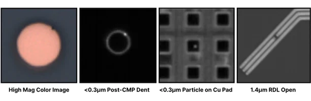

The semiconductor industry is currently navigating a paradigm shift as advanced packaging transitions from a secondary manufacturing step to a primary driver of device performance. As chipmakers move toward heterogeneous integration—stacking chiplets, high-bandwidth memory (HBM), and hybrid-bonded components—the economic stakes have risen exponentially. In this high-value environment, the traditional approach to quality control is no longer sufficient. Because value is accumulated incrementally throughout the packaging process, an undetected defect at an early stage can jeopardize an entire assembly worth thousands of dollars. As feature sizes shrink to mirror the rigor of front-end fabrication, manufacturers are finding that they must achieve unprecedented levels of precision, sensitivity, and throughput to maintain yield.
The Evolution of Packaging Complexity
Historically, back-end packaging was considered less demanding than the front-end photolithography and etching processes. However, the industry’s reliance on Moore’s Law—which has effectively slowed in terms of monolithic scaling—has pushed engineers toward advanced packaging as the new frontier for performance gains. This transition began in earnest around 2015 with the commercialization of 2.5D and 3D stacking techniques. Today, the density of microbumps and the fragility of hybrid-bonded interfaces mean that a single micron-scale particle or a minor bonding void can lead to catastrophic failure during operation.
The current technical challenge is multidimensional. Unlike front-end wafer fabrication, where the surface is generally planar, advanced packaging involves diverse topography. Inspection systems must now contend with sidewalls, deep trenches, microbumps, and embedded structures. A defect that is harmless on a flat silicon substrate can be a critical failure point when it resides on a bump-to-bump interface. Consequently, the industry is moving toward a strategy of "complementary metrology," where multiple sensing modalities are unified into a single, high-throughput workflow.
The Mechanics of Integrated Process Control
To address these challenges, modern process control strategies rely on a tiered approach that aligns specific inspection tools with the risks inherent to each manufacturing stage.
High-sensitivity 2D optical inspection serves as the first line of defense, identifying surface-level contaminants and pattern anomalies. However, as packaging reaches 3D architectures, 2D imaging is inherently limited. To visualize internal defects—such as subsurface delamination, voids within the molding compound, or misalignment in TSV (Through-Silicon Via) stacks—engineers are increasingly utilizing high-speed infrared (IR) inspection. IR light penetrates opaque materials, allowing for non-destructive characterization of the internal state of a package.

When combined with 3D metrology, which provides high-precision volumetric data on bump height and surface coplanarity, these tools create a comprehensive "digital twin" of the package at each layer. This unified data flow is critical. If a manufacturer only measures bump height without checking for subsurface voids, they may pass a device that is geometrically correct but structurally compromised. By integrating these datasets, engineers can make informed, data-driven decisions at every process gate.
Productivity and the Throughput Bottleneck
A primary concern for high-volume manufacturing (HVM) is the "productivity trap." In the past, increasing sensitivity often meant sacrificing scan speed. For a facility churning out thousands of units per hour, an inspection tool that slows the line is not just a technological failure; it is a financial one.
Modern inspection architectures are mitigating this through purpose-built imaging. By utilizing multi-angle illumination, systems can now highlight sidewall defects and low-contrast anomalies in a single pass. This reduces the need for multiple re-scans and allows for the detection of defects that would have previously been obscured by the reflective nature of metal bumps or the diffuse scattering of organic substrates. By optimizing the optical path and increasing the raw data throughput of the sensors, vendors are enabling manufacturers to maintain "in-line" speeds while achieving the sensitivity levels required for sub-micron feature sizes.
The Challenge of Nuisance Classification
As inspection tools become more sensitive, they inevitably flag a larger number of "events." A significant hurdle for modern fab engineers is the high rate of nuisance detections—defects that are identified by the machine but have no impact on the functional performance of the device.
Distinguishing between a critical yield-killer and a benign nuisance is one of the most difficult tasks in modern metrology. Without advanced classification algorithms, engineers can spend hours manually reviewing thousands of images, leading to "alert fatigue" and increased time-to-decision. Industry leaders are now integrating machine learning and artificial intelligence into the inspection workflow to automate this classification. By training models on historical yield data, the software can automatically categorize defects based on their severity and location, allowing human operators to focus only on those events that necessitate immediate process intervention.
Implications for the Semiconductor Supply Chain
The implications of these advancements extend beyond simple yield improvement. They represent a fundamental change in the manufacturing philosophy of the semiconductor industry. By shifting from a "detect and discard" mentality to a "detect and predict" strategy, manufacturers are reducing the scrap rate of high-value components.

For instance, the CMP (Chemical Mechanical Planarization) process for hybrid bonding is a critical point of failure. Even a sub-nanometer variation in surface roughness can prevent a successful bond. By deploying real-time metrology that feeds back into the CMP tool parameters, manufacturers can adjust the process on the fly, preventing the creation of defective parts before they even reach the bonding stage. This proactive approach is essential for maintaining the economic viability of chiplet-based architectures.
Future Perspectives
Looking forward, the industry is expected to push this integration even further. The next logical step, according to industry analysts, is the convergence of front-end and back-end data. If a defect is detected on the wafer edge during the fabrication phase, that information should be tracked and correlated with the performance of that same wafer during the packaging assembly phase.
This "cradle-to-grave" traceability is the holy grail of semiconductor manufacturing. By linking the entire process history of a single chiplet, manufacturers can identify the root causes of failure with far greater accuracy. As we move into the era of 2-nanometer nodes and beyond, the margins for error will continue to shrink. The companies that successfully implement a unified, multi-modal, and intelligent inspection platform will be the ones that define the next decade of silicon innovation.
In summary, the demand for higher performance is forcing the industry to reconcile the conflicting requirements of extreme sensitivity and high-volume productivity. Through the adoption of integrated platforms that synthesize optical, infrared, and 3D data, manufacturers are effectively closing the loop on process control. This evolution not only protects the massive investment required for advanced packaging but also serves as the foundation for the next generation of computing, communication, and artificial intelligence hardware. The transition toward intelligent, unified inspection is no longer optional; it is the prerequisite for scaling the complexity of modern semiconductor devices.
