

The global semiconductor industry has entered a transformative phase characterized by massive state-led investments, a pivot toward specialized artificial intelligence (AI) hardware, and a strategic reshuffling of the global supply chain. In a series of high-stakes announcements, South Korea has unveiled a comprehensive national strategy to dominate the AI-semiconductor nexus, while European and Japanese giants have reached critical milestones in power semiconductor and memory production. These developments signal a shift from general-purpose computing toward a highly integrated ecosystem where physical robotics, energy-efficient power management, and next-generation memory architectures are prioritized to meet the insatiable demands of the AI era.
South Korea’s Tri-Partite Strategy for AI Sovereignty
The South Korean government has officially launched an ambitious industrial roadmap designed to secure its position as a global "AI G3" powerhouse. The strategy, centered on three "Mega Projects," seeks to unify the country’s world-leading semiconductor manufacturing capabilities with the emerging fields of physical AI and localized data center infrastructure. By integrating these sectors, Seoul aims to create a self-sustaining loop where domestic chips power domestic robots and AI services, which in turn drive further semiconductor innovation.
The first pillar of the initiative focuses on the establishment of massive regional chip clusters. These clusters are designed to go beyond mere fabrication, incorporating advanced packaging capacity—a segment of the supply chain where South Korea has traditionally trailed behind Taiwan’s TSMC. The government has pledged comprehensive support for the necessary "hard" infrastructure, including dedicated power grids, high-capacity water supply systems, and shovel-ready industrial sites.
The second pillar targets "Physical AI," specifically robotics and autonomous systems. By incentivizing the development of on-device AI chips tailored for mechanical movement and environmental sensing, South Korea hopes to lead the transition from digital AI (chatbots and software) to embodied AI (industrial and service robots). The third pillar involves the deployment of AI-specific data centers that utilize domestically produced, high-bandwidth memory (HBM) and low-power AI accelerators, reducing reliance on foreign cloud providers.
Industry analysts suggest that this "All In" approach is a direct response to the U.S. CHIPS Act and China’s aggressive domestic subsidization. By streamlining workforce development and regulatory hurdles, South Korea is attempting to compress a decade of industrial evolution into the next few years.
Europe’s Power Play: The Infineon Smart Power Fab in Dresden
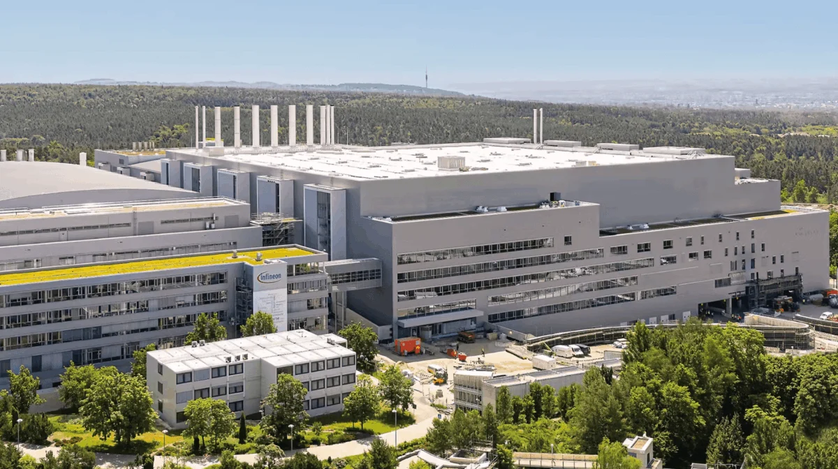
In a significant victory for the European Union’s technological sovereignty, Infineon Technologies AG has inaugurated its "Smart Power Fab" in Dresden, Germany. The $5.7 billion (€5 billion) facility was completed several months ahead of schedule, a rarity in large-scale semiconductor construction. This plant is now the world’s largest and most advanced production site for intelligent power semiconductors and analog/mixed-signal technologies.
The Dresden facility, situated within the "Silicon Saxony" cluster, is expected to create 1,000 high-tech jobs. Its primary output will be chips used in power management applications—the "muscles" of modern electronics. These components are essential for the green transition, found in everything from electric vehicle (EV) drivetrains and renewable energy inverters to the power supply units of AI data centers.
"This investment is a milestone for the decarbonization and digitalization of our society," an Infineon spokesperson noted during the opening ceremony. The facility utilizes 300mm thin-wafer technology, which significantly improves efficiency and reduces material waste compared to older manufacturing processes. The early completion of the Dresden fab underscores Europe’s ability to execute complex industrial projects when state support—via the European Chips Act—aligns with private corporate strategy.

Advancements in Memory and Storage: Japan and Beyond
While Europe secures the power management market, Japan is reinforcing its stronghold on the global storage market. Kioxia Corporation and SanDisk (a Western Digital brand) have officially commenced production of their 10th-generation 3D flash memory products at the Kitakami Fab 2 plant.
This new generation of NAND flash features a significantly higher layer count and bit density, allowing for higher-capacity storage in smaller form factors. As AI models grow in complexity, the need for rapid data retrieval from storage to memory becomes a bottleneck; Kioxia’s latest innovation aims to alleviate this "memory wall" by providing the high-speed data pipelines required for training large language models (LLMs).
Simultaneously, the automotive sector is securing its own future. General Motors (GM) has reportedly moved to secure long-term memory supply chains, recognizing that the software-defined vehicles of the future will require memory buffers comparable to high-end workstations. This move reflects a broader trend of "vertical integration by proxy," where original equipment manufacturers (OEMs) bypass traditional Tier-1 suppliers to deal directly with semiconductor foundries and memory makers.
Technological Innovations in RF and Power Management
The technical landscape is seeing a surge in specialized tools designed to reduce the risk of "tapeout" failure—the final stage of the design process before a chip goes to manufacturing. Keysight Technologies and Win Semiconductors have released a joint Monolithic Microwave Integrated Circuit (MMIC) design workflow. This integrated environment connects on-chip multi-domain simulation with off-chip evaluation board design.
Targeted at 5G/6G base stations and satellite communications, this workflow allows Gallium Nitride (GaN) design houses to achieve success on their first manufacturing pass. GaN is increasingly favored over traditional silicon for high-frequency applications due to its ability to handle higher voltages and temperatures.
In the data center space, Toshiba has launched a new 80V N-channel power MOSFET. Fabricated using the latest U-MOS11-H process, this component is designed specifically for switched-mode power supplies. As AI data centers consume unprecedented amounts of electricity, even fractional improvements in the efficiency of power MOSFETs can result in millions of dollars in energy savings across a global server fleet.
Frontier Research: From Carbon Nanotubes to Reconfigurable Semiconductors
Academic and corporate research labs are pushing the boundaries of material science to solve the heat and efficiency challenges of modern computing. A team led by the Korea Advanced Institute of Science and Technology (KAIST) has demonstrated a monolithic 3D-integrated, all-solid ion-gated carbon nanotube transistor. This device can tune ionic conductance for reservoir computing, a type of neuromorphic hardware that mimics the human brain’s temporal data processing. Such technology could lead to ultra-compact AI hardware that processes data with a fraction of the energy used by current GPUs.
At Princeton University, researchers have reported a method for making large-area 2D semiconductors photo-programmable. By using chromic molecular layers, the team can modify a material’s electronic properties with light after it has been fabricated. This opens the door to reconfigurable semiconductor devices that can be "reprogrammed" at the hardware level to perform different tasks, effectively creating a "liquid" architecture for AI.
Meanwhile, a study from the Massachusetts Institute of Technology (MIT) has provided a nuanced view of the AI energy crisis. The researchers found that the flexibility of data center energy use—the ability to shift loads based on grid demand—is more critical than the total amount of electricity consumed. This finding is expected to influence how future AI clusters are integrated into national power grids.

The Shift to Post-Quantum Cryptography (PQC)
As semiconductor hardware advances, the security frameworks protecting them are undergoing a radical overhaul. The U.S. National Security Agency (NSA) and the Department of the Army (DEVCOM) have launched the "QuantumEAGLe Initiative." This program focuses on securing the U.S. quantum supply chain and developing commercial roadmaps for quantum-resistant technologies.
Microsoft has also accelerated its "Quantum Safe Program," announcing a goal to transition all its products and services to Post-Quantum Cryptography (PQC) by 2029. This timeline is significantly more aggressive than previous industry estimates and aligns with government mandates in the U.S. and France, which have set 2030 as the deadline for critical infrastructure operators to become PQC-compliant. The urgency stems from the "harvest now, decrypt later" threat, where adversaries collect encrypted data today with the intent of decrypting it once viable quantum computers emerge.
Workforce Dynamics: Burnout and the New "AI Philosophers"
The rapid pace of the AI revolution is taking a significant toll on the human capital driving it. Reports from Silicon Valley indicate a surge in "AI burnout," with engineers working 16-hour days and sleeping in offices to keep up with accelerated development cycles. The expectation to manage multiple "AI agents" around the clock has, in many cases, increased the workload rather than easing it.
In response to the long-term talent shortage, Micron has announced a $250 million investment to support the next generation of workers through the U.S. government’s new 530A accounts, which provide long-term savings opportunities for children and families. This move is seen as a strategic effort to build a "cradle-to-fab" pipeline of talent.
The nature of semiconductor and AI jobs is also evolving. The Economist recently highlighted a growing demand for "AI Philosophers"—specialists tasked with defining the ethical boundaries and logic structures of autonomous systems. Furthermore, international cooperation is expanding, with Vietnam and Germany signing new agreements to jointly develop a high-tech workforce capable of supporting the next generation of semiconductor fabs.
Broader Impact and Industry Outlook
The convergence of South Korea’s massive state planning, Europe’s specialized manufacturing, and the global rush toward quantum-safe security indicates that the semiconductor industry is no longer just a cyclical business—it is the foundation of national security and economic survival.
The successful early opening of Infineon’s Dresden fab suggests that localized manufacturing is viable when supported by robust policy. However, the warnings from regions like Oregon—where officials recently cautioned that their semiconductor cluster is becoming vulnerable to aggressive competition from other states—highlight the volatility of this new era. As the industry moves toward the 2026–2030 window, the winners will likely be those who can balance rapid technological scaling with energy flexibility and human-centric workforce policies.
