
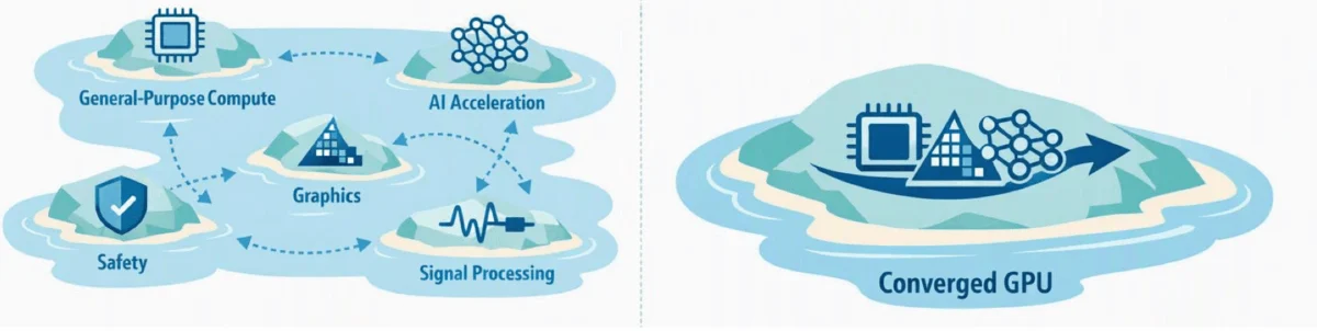

The 2026 TSMC North America Open Innovation Platform (OIP) Ecosystem Forum in Santa Clara has served as the definitive stage for the semiconductor industry’s latest technological pivots, highlighting a significant transition toward heterogeneous integration and the practical deployment of quantum computing. As the industry moves past the limitations of traditional scaling, the event underscored a collective focus on specialized architectures—shifting from the monolithic GPU models of the past toward an "accelerator archipelago" where diverse compute resources are tightly coupled through advanced packaging and photonics.
The Shift Toward Accelerator Architectures
The centerpiece of the forum was the discourse surrounding the evolution of hardware acceleration. Industry leaders, including representatives from Imagination Technologies, presented schematics illustrating the departure from general-purpose converged GPUs toward highly specialized, disaggregated compute fabrics. This architectural shift is not merely a design preference but a requirement for modern AI workloads, which demand lower latency and higher energy efficiency than standard silicon architectures can currently provide.
By fragmenting the compute workload across multiple specialized units, manufacturers are effectively reducing the thermal and power bottlenecks that have plagued data center-grade chips over the last three years. This trend is further supported by the industry’s rapid adoption of advanced packaging, which allows for the integration of disparate die types—such as memory, logic, and optical interconnects—within a single package.
Quantum Computing Reaches Practical Benchmarks
The landscape of quantum computing underwent a notable shift this week, moving from purely theoretical research to functional, error-corrected implementations. A primary development involves the work of researchers from the University of Pavia, CEA-Leti, and STMicroelectronics, who successfully demonstrated a fully integrated quantum frequency processor on a silicon chip. This achievement is a critical milestone, as it bridges the gap between traditional silicon-photonics platforms and the sensitive requirements of quantum-state generation and programmable spectral control.
Concurrent with this, Microsoft’s decision to provide DARPA with access to its topological qubits, built on the Majorana 2 chip, marks a maturation point in quantum testing. By allowing independent evaluation at a specialized facility in Maryland, the industry is moving toward standardized benchmarking—a prerequisite for the eventual commercialization of fault-tolerant quantum systems.
In parallel, IonQ’s announcement regarding its real-time quantum error-correction decoder represents a significant breakthrough in operational efficiency. By running the decoder on a standard, off-the-shelf CPU with a latency penalty of just 0.02%, IonQ has addressed one of the most persistent "pain points" in quantum development: the overhead required to manage qubit decoherence. Furthermore, the German-backed NFQC-1k project, which aims to develop a 1,000-qubit trapped-ion system with a €122 million investment, signals that national governments are now moving to secure domestic supply chains for quantum hardware, viewing it as a strategic asset comparable to classical semiconductor manufacturing.
Advanced Materials and Physical AI
Research into the physical underpinnings of computing has also seen accelerated progress. A collaboration between Los Alamos National Laboratory (LANL) and the University of Pisa has shed light on self-organizing networks of nanowires and nanoparticles. This "physical AI" approach—where the hardware itself adapts its electrical connections to learn and process information—could revolutionize edge computing.
As UCLA’s Adam Stieg noted, the ability for hardware to operate locally and adapt to environmental changes is essential for the next generation of autonomous vehicles and satellites. By moving the learning process from software-heavy cloud layers to the hardware level, these devices can operate with significantly reduced energy consumption and improved response times, effectively decentralizing the intelligence currently concentrated in massive data centers.
Workforce Development and Regulatory Environment
The technical advancements discussed at the forum are being met with a concerted effort to cultivate the next generation of semiconductor engineers. The joint initiative between the University of Illinois Urbana-Champaign and Purdue University serves as a model for this effort, focusing on the end-to-end lifecycle of chip production—from initial design and material science to advanced packaging and testing.
However, this academic push occurs within a complex regulatory framework. The current administration’s directive to link H-1B visa approvals to domestic layoff data adds a layer of uncertainty for companies that rely on international talent to staff their high-tech R&D divisions. By mandating that agencies consider company-wide workforce stability when reviewing visa petitions, the federal government is attempting to prioritize domestic labor absorption. This policy, combined with the continued $100,000 salary threshold for H-1B holders, creates a more stringent and expensive environment for talent acquisition, forcing firms to balance their need for specialized expertise against the rising administrative burden of international hiring.
In the public sector, New York State’s $5 million investment in a STEM hub at Cicero-North Syracuse High School highlights the localized approach to workforce preparation. By aligning local educational infrastructure with the planned Micron fabrication facilities in Central New York, the state is attempting to create a self-sustaining pipeline of technical talent that can meet the long-term demands of a modern semiconductor fab.
Addressing the Test Data Bottleneck
A critical theme underscored by Siemens EDA’s expert, Vidya Neerkundar, is the mounting challenge of test data management. As chip designs increase in complexity, the volume of data generated during the testing phase has outpaced the capabilities of legacy infrastructure. The industry is now grappling with how to move this data through the system without inducing significant delays in manufacturing throughput.
The solutions being proposed involve a shift toward more intelligent, standards-based test processes that can handle the intricacies of multi-die and advanced packaging designs. This is not just a logistical hurdle; it is a financial one. As yield rates directly impact the profitability of advanced nodes, the ability to conduct rapid, comprehensive testing—and to do so using optimized standards—has become a competitive differentiator for firms across the semiconductor ecosystem.
Strategic Outlook and Upcoming Industry Milestones
The remainder of the fourth quarter of 2026 is densely packed with events that will likely define the trajectory of these technologies. From the IMAPS Symposium in Boston to the OCP Global Summit in San Jose, the industry is entering a phase of rapid information exchange.
The focus on "Agentic AI" at the upcoming Rambus Design Summit and the emphasis on "Bridging Design and Manufacturing with AI" at the ESD Alliance session during SEMICON West suggest that the industry is moving beyond the hype cycle of AI and into a period of deep, functional integration. The objective for the coming months is clear: to reconcile the massive hardware requirements of next-generation AI with the constraints of power, thermal management, and talent availability.
The integration of photonic chips, the standardization of quantum error correction, and the localized training of the semiconductor workforce are not isolated events. Rather, they represent the three pillars of the next industrial era: efficient compute, breakthrough processing power, and the human capital necessary to sustain it. As these trends converge, the reliance on forums like the TSMC OIP Ecosystem will only grow, serving as the essential meeting point for a global industry undergoing a fundamental transformation.
While the geopolitical and regulatory hurdles remain significant, the sheer velocity of research and development in materials science and architectural design suggests that the industry is well-positioned to navigate these challenges. The transition from "monolithic" to "archipelago" is effectively underway, marking the end of a long era of predictable, scaling-based progress and the beginning of an era defined by ingenuity in integration and architectural specialization.
