
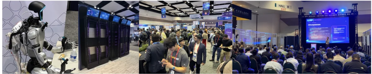

The global semiconductor landscape is currently undergoing a period of intense transformation characterized by rapid advancements in AI infrastructure, aggressive regional expansion, and a fundamental shift in how computing hardware is designed and verified. From the recent AI Infra Summit in Santa Clara to the latest developments in quantum error correction and 2nm manufacturing, the industry is balancing the immediate, massive demand for generative AI hardware with long-term goals for workforce development and sustainable manufacturing.
The AI Infrastructure Imperative
The AI Infra Summit, held recently in Santa Clara, served as the epicenter for discussions regarding the future of the data center. The primary narrative emerging from the event was not merely about raw compute power, but about the holistic optimization of the AI stack. Industry leaders emphasized that the bottleneck for large-scale AI deployment has shifted from simple chip performance to the interplay between memory bandwidth, interconnect latency, and power efficiency.

Discussions at the summit highlighted a critical shift toward "system-level" design. As AI models scale into the trillions of parameters, the physical distance between memory and processing units has become a primary constraint. Engineers are increasingly looking toward 3D packaging and advanced chiplet architectures to minimize data movement, which currently consumes a significant portion of total system energy. Furthermore, the focus on Root of Trust (RoT) solutions for AI System-on-Chips (SoCs) has intensified, as data centers must now treat security as a foundational element of the hardware architecture rather than a software-side afterthought.
Global Manufacturing and Capacity Expansion
North America remains the primary theater for large-scale semiconductor capacity expansion, driven by federal incentives aimed at de-risking the global supply chain. Recent reports indicate that the push for domestic production is extending beyond traditional logic chips, encompassing a broader push for advanced packaging and high-bandwidth memory (HBM) facilities.
Concurrent with North American efforts, India has emerged as a significant player in the global build-out. By incentivizing the creation of local assembly, testing, marking, and packaging (ATMP) facilities, the Indian government is attempting to integrate itself into the mid-to-late stages of the semiconductor value chain. While current efforts are focused on mature nodes, the long-term objective remains the establishment of a comprehensive ecosystem that can support complex IC design and eventual fabrication.

Meanwhile, in Asia, Chinese equipment manufacturers are steadily gaining market share. Despite stringent export controls on advanced lithography tools, local firms have shown unexpected resilience, particularly in the legacy and mid-range node segments. This growth is forcing a recalibration of global supply chain strategies, as companies look to diversify their sourcing to mitigate potential geopolitical disruptions.
Advanced Nodes and the 2nm Transition
The race toward 2nm and below continues to define the cutting edge of semiconductor manufacturing. The transition to Gate-All-Around (GAA) transistor architectures is proving to be a complex engineering milestone. Unlike the move from FinFET to GAA, which was primarily a structural change, the shift to 2nm involves a deeper integration of new materials and advanced backside power delivery networks.
Manufacturing partners are currently finalizing their process design kits (PDKs) for these nodes, with early production runs expected to prioritize high-performance computing (HPC) applications. The complexity of these nodes has led to a significant increase in design costs, further emphasizing the need for robust electronic design automation (EDA) tools capable of handling the massive data volumes associated with sub-2nm verification.

Innovations in Research and Computing
Academic and government-led research continues to provide the roadmap for the next generation of computing. Notably, researchers at the National University of Singapore (NUS) have developed a reconfigurable transistor utilizing atomically thin molybdenum disulfide (MoS2) and ferroelectric hafnium zirconium oxide (HZO). This device can function as a logic gate, an artificial synapse, or a neuron, potentially allowing for hardware that can adapt its function based on the workload—a significant step toward neuromorphic computing.
In the United States, a $5.5 million DARPA-funded project led by USC is exploring the use of magnetic spin waves to process information. By moving away from electron charge, this research aims to drastically reduce the heat generated by transistors, which is a major barrier to further scaling. If successful, this technology could offer a low-power alternative to traditional CMOS logic, particularly for edge AI applications where energy constraints are paramount.
Quantum Computing: From Theory to Fault Tolerance
The quantum computing sector has moved into a new phase, focusing on fault tolerance rather than just qubit counts. The U.S. Department of Energy (DOE) has launched a $215 million initiative to foster the development of quantum systems capable of performing hundreds of millions of fault-tolerant operations. This shift marks a transition from experimental "Noisy Intermediate-Scale Quantum" (NISQ) devices to practical, scalable quantum infrastructure.

Industry players are also making strides in integration. Quobly’s recent demonstration of quantum operations on a silicon chip—leveraging standard FD-SOI transistors—suggests that the industry may be able to utilize existing semiconductor manufacturing infrastructure to build quantum processors. This synergy between traditional silicon fabrication and quantum hardware is viewed as a crucial step toward commercial viability.
The Workforce and Economic Landscape
The semiconductor industry is currently grappling with a dual challenge: the rapid pace of technological innovation and the scarcity of specialized talent. While federal initiatives, such as the U.S. Department of Energy’s $16 million prize for critical minerals workforce training, are attempting to bridge the gap, the industry continues to face bottlenecks.
A recent judicial development regarding F-1 and J-1 visa statuses has introduced a degree of uncertainty for international students and researchers in the STEM fields. Because a large percentage of the U.S. semiconductor workforce pipeline relies on foreign-born talent currently in the U.S. for education, the stability of these visa pathways is essential for maintaining the momentum of domestic chip builds. The temporary postponement of the DHS rule eliminating "duration of status" provides a reprieve, but it highlights the volatility of the talent supply chain.

Analysis of Current Market Trends
Looking at the broader economic picture, McKinsey and other analysts have identified several key trends for the coming years:
- Vertical Integration: Companies are increasingly looking to own more of the stack, from custom silicon design to data center management.
- Sustainability as a Design Metric: Power efficiency is no longer just an operating expense; it is a design constraint that dictates the success of new chip architectures.
- Regionalization: The era of a single, globalized semiconductor supply chain is being replaced by a multipolar model, where regional hubs aim for a degree of self-sufficiency.
Conclusion and Looking Ahead
As we move into the final quarter of 2026, the semiconductor industry is defined by the convergence of AI, quantum, and traditional silicon manufacturing. The sheer volume of events, ranging from the OCP Global Summit to SEMICON West, underscores an industry that is operating at a breakneck pace. The core task for stakeholders in the coming months will be to balance the immediate, insatiable appetite for AI-capable hardware with the need for long-term sustainability, both in terms of energy usage and human capital.
The successful transition to 2nm nodes, the maturity of quantum fault tolerance, and the stabilization of global supply chains will dictate the winners of the next decade. For now, the emphasis remains on iterative, high-stakes progress, where each marginal gain in transistor density or power efficiency provides a critical competitive advantage in an increasingly digitized global economy.
