
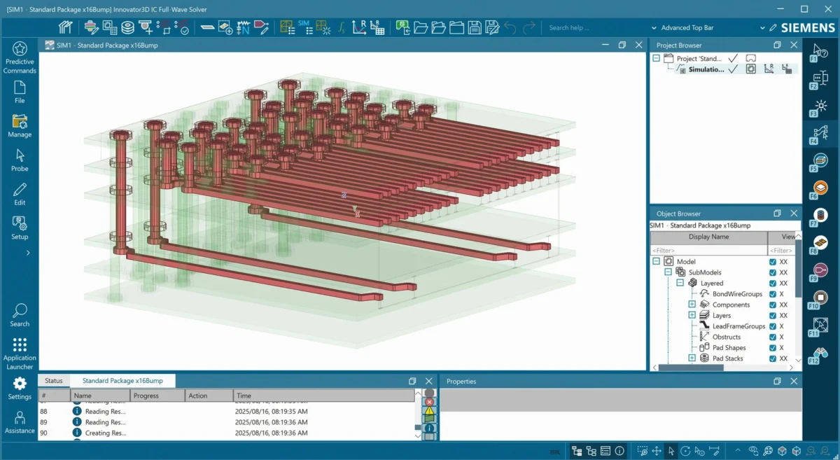

The semiconductor industry is currently undergoing a seismic shift as traditional monolithic System-on-Chip (SoC) designs reach the physical and economic limits of Moore’s Law. As a result, the transition toward heterogeneous integration—specifically 2.5D and 3D Integrated Circuits (3D-ICs)—has become the primary pathway for scaling performance in high-performance computing, artificial intelligence, and mobile technologies. However, this transition introduces unprecedented design complexities, particularly regarding the thousands of connections between chiplets, interposers, and package Ball Grid Arrays (BGAs). To address these challenges, designers are adopting sophisticated methodologies that prioritize pre-planning, predictive analysis, and rigorous protocol compliance, specifically focusing on the Universal Chiplet Interface Express (UCIe) standard.
The Complexity of Heterogeneous Interconnects
In a modern 3D-IC environment, the density of interconnects is staggering. A single package may house multiple chiplets from different process nodes, all requiring seamless communication through an interposer or substrate. The traditional methodology of manual or automatic routing without exhaustive pre-planning is increasingly proving inadequate. In such legacy flows, designers often encounter "bump field blockages," where the physical arrangement of microbumps prevents efficient signal escape. This leads to route congestion, channel blockages, and ultimately, a failure to meet stringent interface protocol specifications.

The consequences of these failures are severe. When signal performance or protocol compliance is not met during the late stages of design, engineers are forced into "rip-up and retry" iterations. These cycles are not only time-consuming but also compromise the integrity of the final product. Excessive via usage, increased route lengths, and signal integrity issues such as crosstalk and attenuation become prevalent, potentially delaying time-to-market by months and inflating development costs.
Chronology of the 3D-IC Design Lifecycle
To mitigate these risks, the 3D-IC design flow has evolved into a structured, multi-stage process. The first stage involves the creation of a 3D digital twin—a comprehensive virtual representation of the entire assembly. This is followed by pathfinding, where designers explore optimal floorplans for chiplets and interposers. The industry is currently focused on the third and most critical phase: finalizing the design scenario and moving toward sign-off.
This stage acts as the bridge between theoretical architecture and physical reality. It involves a rigorous set of steps:

- Interface Compliance Verification: Ensuring high-speed serial links meet standards before detailed routing.
- Multiphysics Optimization: Analyzing the interaction of thermal, mechanical, and electrical forces.
- Comprehensive Test Planning: Integrating Design-for-Test (DFT) strategies at the stack level.
- Netlist Synchronization: Resolving any logical versus physical connectivity anomalies.
- Formal Sign-off: Using industry-standard tools to verify the assembly against foundry rules.
Achieving UCIe Protocol Compliance
A significant portion of modern 3D-IC development centers on the Universal Chiplet Interface Express (UCIe). As an open specification for die-to-die interconnects, UCIe has become the de facto standard for logic-to-logic communication. Achieving compliance with this protocol requires a proactive approach known as signal integrity pathfinding.
Before a single trace is routed, designers must explore physical interconnect structures. This involves analyzing substrate materials, layer stackups, and chiplet bump arrays. If a chiplet is sourced from a third party, its bump array is often fixed, requiring the package designer to model the associated serial link breakout patterns with extreme precision. The goal is to minimize return loss and insertion loss—the two primary enemies of high-speed data throughput.
Advanced tools now allow for the automated generation of 3D electromagnetic (EM) models. These models, created via full-wave or hybrid field solvers, enable designers to simulate various "case study" scenarios. By utilizing both standards-based compliance analysis and vendor-specific IBIS-AMI (Input/Output Buffer Information Specification – Algorithmic Modeling Interface) models, design teams can predict real-world performance. This dual approach ensures that the chiplets not only meet the UCIe standard for interoperability but are also optimized for the specific characteristics of the vendor’s physical layer (PHY).

The Role of Predictive Multiphysics Analysis
In the realm of 2.5D and 3D integration, the physical coupling of components is so tight that electrical behavior cannot be divorced from thermal and mechanical effects. As active dies are stacked or placed in close proximity, heat accumulation becomes a primary concern. This can lead to "thermal runaway," where heat degrades electrical performance, which in turn generates more heat.
Furthermore, the varying thermal expansion rates of different materials—silicon, organic substrates, and copper interconnects—can cause mechanical stress. This stress often manifests as die warping or the fracturing of microbumps and Through-Silicon Vias (TSVs). Industry data suggests that postponing multiphysics analysis until the physical implementation phase increases the risk of costly redesigns by over 40%.
Modern design environments, such as the Siemens Innovator3D IC platform, emphasize "shift-left" analysis. By providing physics-driven feedback during the Register Transfer Level (RTL) and floorplanning stages, designers can make informed choices about materials and cooling solutions before constraints are locked in. This continuous evaluation ensures that every change to the floorplan is vetted for its impact on system reliability and manufacturing yield.

Advanced Testing and Stack-Level DFT
Testing a 3D-IC is significantly more complex than testing a traditional 2D chip. While die-level testing remains essential to ensure "known-good-die" (KGD) status, the assembly process introduces new potential defects in the die-to-die interconnects.
The industry is moving toward a hierarchical DFT principle that includes a "stack-level" hierarchy. In this model, test patterns are generated once at the core level and then retargeted. For wafer-level testing, patterns are mapped to the die top; for post-packaging testing, they are mapped to the top of the entire stack. This efficiency is vital, as it avoids the need to reload the entire stack’s data for every test iteration.
However, designers must also account for unintended DFT effects. For instance, the heat generated during the testing of one die can cause a false failure in an adjacent die due to thermal sensitivity. Effective DFT solutions must allow for the composition of stack-level patterns that optimize for power consumption and heat dissipation during the test cycle itself.

Verification, Sign-off, and the Verification Gap
The final hurdle in the 3D-IC journey is formal sign-off. Historically, there has been a "verification gap" in IC-package co-design because traditional tools were built for either the die or the package, but rarely both. Advanced packages blur these lines, requiring a unified flow.
Designers must first perform Design Rule Checks (DRC) and Layout Versus Schematic (LVS) verification. This process is complicated by the vertical nature of 3D-ICs. Traditional tools often interpret geometries on different levels as being co-planar, leading to false errors. To solve this, tools like Calibre 3DStack provide a designer-centric approach that is agnostic to technology nodes and manufacturing vendors. It allows for the independent verification of complex multi-substrate assemblies, ensuring that chiplet alignment and connectivity match the "golden" system netlist.
To further validate the manufacturing process, design teams often create "test vehicles." These are specialized versions of the design that use daisy-chain structures instead of functional netlists to verify the physical integrity of the layers and placements. Automating the creation of these structures is essential for reducing human error and accelerating the move to high-volume production.

Broader Implications for the Semiconductor Ecosystem
The shift toward standardized 3D-IC design flows has profound implications for the global semiconductor ecosystem. It enables a more modular "chiplet marketplace," where companies can mix and match components from different foundries with confidence that they will integrate successfully. This modularity is expected to reduce the entry barrier for custom silicon, allowing smaller players to innovate in specialized fields like edge AI and automotive sensors.
Furthermore, the collaboration between Electronic Design Automation (EDA) providers, foundries, and Outsourced Semiconductor Assembly and Test (OSAT) providers is reaching new heights. The release of comprehensive Package Assembly Design Kits (PADKs) is a testament to this cooperation, providing the necessary rules and models to ensure that heterogeneously integrated designs are both manufacturable and reliable.
As the industry moves toward the next phase—detailed substrate implementation and tape-out—the groundwork laid during the scenario sign-off phase remains the most critical factor in project success. By embracing predictive analysis, multiphysics co-design, and standardized protocols like UCIe, the semiconductor industry is successfully navigating the complexities of the 3D-IC era, ensuring that the next generation of computing is more powerful, efficient, and reliable than ever before.
