

A chiplet can be fully characterized, tested, and considered a "known good die," but in the era of heterogeneous integration, none of those metrics guarantee the component will maintain its performance after integration into a complex package. As the semiconductor industry pivots toward advanced packaging architectures—utilizing 2.5D and 3D stacking—the traditional boundaries of chip design have dissolved. Engineers are no longer merely designing a single monolithic silicon die; they are managing a multi-physics environment where the mechanical, electrical, and thermal properties are in constant flux. The industry’s solution, the digital twin, is struggling to keep pace with the reality of manufacturing, as the "as-designed" model frequently diverges from the "as-manufactured" product.
The Myth of the Static Component
For decades, semiconductor design operated on the premise that if a die was validated at the wafer level, it was ready for assembly. However, the introduction of chiplets has fundamentally altered this calculus. When a die is removed from its original testing environment and placed onto a different substrate, or encased in a new thermal interface material (TIM), its operational characteristics change.
A thermal path that functioned flawlessly in an initial product SKU may trigger aggressive throttling in a second iteration because the package’s power envelope or cooling assumptions have shifted. This is the primary hurdle facing digital twins for advanced packaging: they must predict how known, discrete components will behave after integration into a larger, unpredictable system. Kenneth Larsen, senior director of product management at Synopsys, highlights this persistent disconnect: "The chiplet has not changed, but its electrical, thermal, and mechanical environment has. Engineers are now dealing with an entirely different system, and the digital twin must account for the cumulative impact of the substrate, the assembly process, and the final thermal management solution."
Fab Twins vs. Package Twins: A Contextual Shift
While digital twins have found success in front-end wafer fabrication, the transition to back-end packaging presents a different set of challenges. A fab process twin typically resides within a controlled, high-volume manufacturing environment. It leverages decades of statistical learning, equipment behavior modeling, and process history. In contrast, a package digital twin must solve a broader, more fragmented integration problem.
The nature of the problem shifts from one of process control to one of system-level orchestration. In advanced packaging, the package is an extension of the system architecture. Consequently, electrical, thermal, and mechanical behaviors cannot be optimized in isolation. While engineers possess sophisticated tools for each of these domains, these tools currently operate as silos. A true package digital twin requires these domains to synchronize around the physical package as it traverses the supply chain from design to assembly, test, and final system deployment.
The Data Hole and Supply Chain Fragmentation
One of the most significant barriers to achieving a functional, end-to-end digital twin is the "data hole." From the perspective of Outsourced Semiconductor Assembly and Test (OSAT) providers, the information required to build an accurate model is often dispersed across the entire ecosystem.
Joon Ahn, vice president of global factory IT and automation at Amkor, notes that an effective digital twin is not a single model, but a connected ecosystem of process, equipment, and supply chain data. "Packaging performance is influenced by interactions among multiple process steps. Some key process information originates upstream in foundry operations or downstream in customer applications," Ahn explains.
Currently, when a die reaches an OSAT, it arrives with wafer-sort results, but rarely with detailed power-density maps or local stress profiles. Substrates arrive within nominal specifications, but often lack data regarding actual warpage across a production lot. This leads to a scenario where downstream analysis appears mathematically precise but remains detached from the manufacturing reality. Furthermore, intellectual property concerns often prevent the free flow of this data. Material suppliers, foundries, and assembly houses operate as distinct entities, each guarding their proprietary processes. This organizational friction makes it difficult to standardize the inputs required for a unified, predictive model.

The Reality of Manufacturing Variability
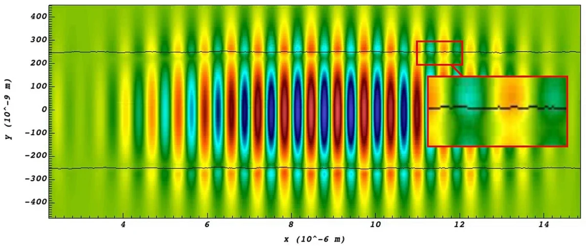
Even if all nominal data were perfectly aligned, manufacturing inherently introduces variability. This is particularly evident in the field of photonics, where small geometric shifts—measured in nanometers—can lead to significant deviations in device performance. Eric Guichard, senior vice president and general manager of Silvaco’s TCAD business unit, notes the growing disconnect between simulation and reality: "A photonic integrated circuit may demonstrate excellent performance in simulation, but high-volume manufacturing introduces variations in dimensions, profiles, and materials that directly affect optical behavior. The design optimized for the ‘as-drawn’ geometry often does not represent the ‘as-manufactured’ device."
This phenomenon extends to the material science domain. Datasets provided by vendors often present static snapshots of properties like Coefficient of Thermal Expansion (CTE) or modulus, measured under idealized conditions. However, materials like polymers and underfills change their characteristics during the curing process. As Brewer Science research scientist Hanlin Chen points out, "Treating these as static numbers causes a lot of simulation-to-silicon gaps." If the digital twin is not updated to reflect how material properties evolve after thermal exposure or assembly, it quickly becomes obsolete.
The Interdependency of Physical Variables
Perhaps the most complex aspect of advanced packaging is that variables rarely act independently. In a sophisticated 3D stack, power distribution, thermal dissipation, and mechanical stress form a tightly coupled feedback loop. Increased current density leads to higher heat, which alters the electrical resistance of the interconnects, further increasing power dissipation.
When separate models are used for these phenomena, the system fails to account for the non-linear interactions that define modern package performance. Standardizing these interfaces is a massive undertaking, as the models for heat transfer and electrical behavior are mature, but the "bridge" models that connect them—where materials, structures, and processes meet—remain poorly defined.
Calibration as a Continuous Process
To remain relevant, a digital twin must be a dynamic entity that undergoes constant calibration. When physical measurements from the assembly line are fed back into the finite-element models, the model evolves. This is becoming a critical practice in high-end applications like hybrid bonding, where experimental distortion data is used to refine future simulations.
However, the industry must resist the urge to measure everything. The cost and throughput implications of measuring every variable at every step are prohibitive. ASE vice president of corporate R&D, CP Hung, suggests a more pragmatic approach: "It’s really about measuring at the points where the package changes state—bonding, molding, curing, and thermal transitions."
By focusing on these "state-change" points, engineers can maintain a high-fidelity model without overwhelming the production line with data collection. This necessitates a "lockstep" approach where model development and physical device manufacturing occur simultaneously. As NLM Photonics CEO Brad Booth observes, "Until I’ve actually built one and shown that it equates to what was in the digital twin, I can’t really say that my digital twin is an accurate representation of the end product."
Implications for the Future
The path forward for digital twins in advanced packaging lies in bridging the gap between design, manufacturing, and operation. A useful package twin cannot be a static artifact created during the design phase; it must be a "living" representation that absorbs real-world data from the assembly line and feeds it back into the design cycle.
The economic implications of success are immense. Companies that can successfully implement end-to-end digital twins will likely see faster time-to-market, higher yields, and improved reliability for their most complex devices. Conversely, those that rely on disconnected, static models risk significant losses due to unforeseen performance degradations once the device reaches the end-user. Ultimately, the goal is to shift from reactive troubleshooting to proactive optimization, ensuring that the digital model remains as reliable as the physical hardware it represents.
