

The semiconductor industry is currently undergoing a structural shift as the era of monolithic system-on-chip (SoC) design gives way to 3D-IC and multi-chiplet heterogeneous integration. While this transition enables the creation of more specialized, high-performance devices, it also introduces an unprecedented level of architectural complexity. As Keith Felton and Todd Burkholder of Siemens Digital Industries Software emphasize, the success of these advanced packages is no longer defined solely by silicon engineering, but by the ability to manage the vast, intricate web of data that underpins them. Without a rigorous framework for data traceability and revision control, the modularity promised by chiplet-based designs risks devolving into a chaotic environment prone to costly errors and protracted design cycles.
The evolution toward 3D-IC design has been rapid. Over the past several years, the industry has moved from theoretical research to high-volume manufacturing of stacked dies. This shift was necessitated by the slowing of Moore’s Law, which forced engineers to seek performance gains through spatial, rather than purely lithographic, scaling. By partitioning a large system into smaller, discrete chiplets—each potentially fabricated on a different process node—manufacturers can optimize for cost, power, and performance at the block level. However, this flexibility creates a new "data management tax." When designers integrate IP from internal libraries, third-party vendors, and open-source ecosystems, the heterogeneity of the design data becomes a significant liability if not properly managed.
A Chronology of Design Complexity
The journey toward modern 3D-IC management can be viewed through a four-part progression established by industry experts throughout 2026. In June, the focus was on the foundational architecture of 3D-IC design, addressing the shift in how engineers conceptualize multi-die assemblies. July followed with a detailed exploration of sign-off methodologies, acknowledging that traditional verification techniques were insufficient for stacked-die environments. August centered on substrate finalization and tapeout, highlighting the critical nature of the physical interface between the chiplets and the underlying packaging.
This current phase, the final pillar of the series, shifts the focus from physical design to information architecture. It addresses the reality that for a design team, an Engineering Change Order (ECO) applied to a single chiplet without proper propagation to the rest of the 3D assembly can lead to catastrophic hardware failure. As systems grow to incorporate dozens of chiplets, the "single source of truth" concept has moved from a best-practice recommendation to a functional requirement for market survival.
The Plethora of IP and the Risk of Fragmentation
In a multi-chiplet ecosystem, a single product might contain logic, memory, and analog IP from half a dozen different sources. Each component arrives with a distinct set of specifications, timing constraints, and physical requirements. If these components are managed in silos, the probability of "version mismatch"—where an engineer inadvertently uses an outdated version of a thermal model or a superseded physical layout—rises exponentially.
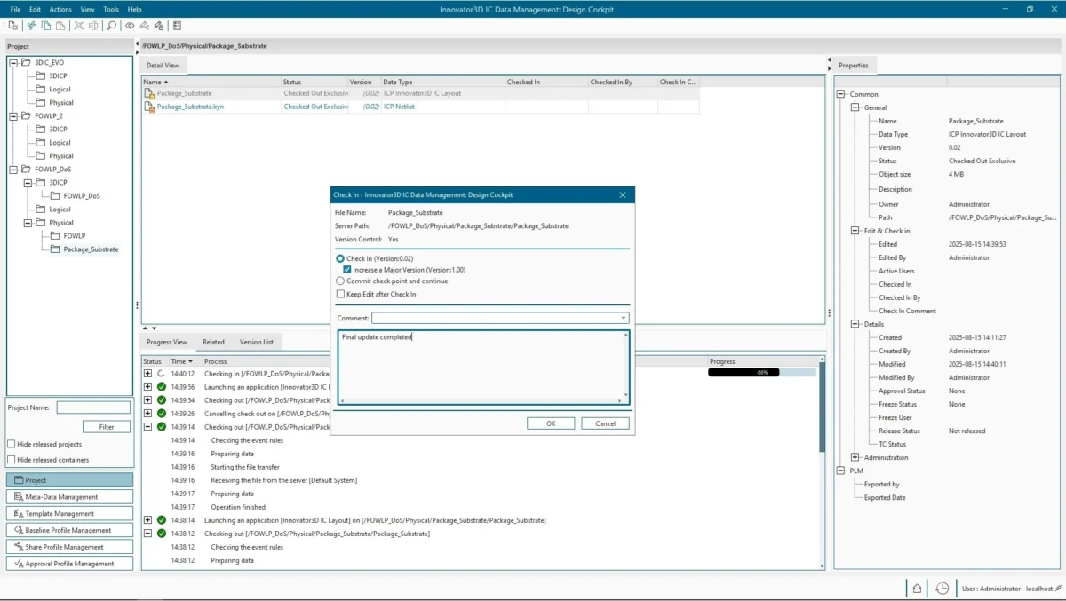
The implications of such errors are not merely academic; they are financial. A single re-spin of a high-end 3D-IC package can cost tens of millions of dollars and delay product delivery by months. To mitigate this, tools like the Innovator3D IC Data Management platform have been developed to act as a centralized cockpit. By treating the entire design as a unified, work-in-progress entity, these systems enforce strict revision control and access rights. This ensures that every member of a globally distributed design team is working against the same master dataset, effectively eliminating the "islands of data" phenomenon that has historically plagued complex SoC projects.
The Necessity of Hierarchical Revision Control
The hierarchy of a 3D-IC design is inherently more complex than that of a traditional SoC. It involves not just the logic within a chiplet, but the interconnects, the interposer, and the substrate that ties the system together. Managing this hierarchy requires a "time machine" approach to data, where every iteration is logged, dated, and linked to a specific design requirement.

Revision control is the backbone of this process. It allows teams to branch off to experiment with specific features or bug fixes without impacting the main design stream. Once a branch is validated, it can be merged back into the production environment with a clear audit trail. This transparency is vital for traceability. If a failure is discovered during post-silicon testing, engineers must be able to trace that failure back to the specific version of the IP used, the specific design iteration, and the specific person who authorized the change. Without this, the root-cause analysis process could take weeks; with it, the diagnostic period is reduced to hours or even minutes.
Centralization as a Strategic Advantage
Distributed design environments are the new standard for the semiconductor industry. It is common for a single design to be split between teams in North America, Europe, and Asia. In such a fragmented landscape, a centralized data hub is the only way to maintain coherence. By providing a single, authoritative repository, companies can ensure that communication gaps do not lead to physical integration failures.
Data gathered from successful implementations suggests that centralized management systems can reduce design cycle times by as much as 20% to 30%. This efficiency gain is achieved primarily by eliminating the time spent verifying that all team members are using the correct data sets and by automating the reporting of design status. When an engineer can pull the latest constraints or layout files instantly, the friction inherent in large-scale collaboration is significantly reduced.
Instant Status Tracking and Analytical Visibility
The final component of a robust data management strategy is the transformation of static data into actionable intelligence. Modern management tools provide real-time dashboards that allow engineering leads to visualize the status of every chiplet in the assembly. This is not just about knowing whether a task is "done" or "in progress"; it is about understanding the impact of that task on the entire system.
For example, if a thermal analysis shows that a specific chiplet is exceeding its power budget, the status-tracking system can immediately flag this to the relevant stakeholders. This proactive approach to project management allows teams to address issues early in the design cycle—the "shift-left" philosophy—when they are still inexpensive to fix. The ability to perform instant status tracking turns data management from a backend administrative task into a competitive advantage that directly influences the quality and reliability of the final product.
Broader Implications for the Semiconductor Industry
The implications of these developments extend beyond individual companies; they affect the entire global supply chain. As we move toward a future where heterogeneous integration becomes the norm, the industry must standardize its approach to data traceability. The "unseen architects" of the semiconductor world—the data management systems—are becoming as important as the EDA tools themselves.
Experts note that as chiplet-based designs permeate everything from data center AI accelerators to consumer mobile devices, the burden of data complexity will only increase. Companies that fail to invest in the infrastructure required to manage this complexity will find themselves unable to compete with the speed and reliability of those who have mastered the art of digital traceability.
In conclusion, the trend toward multi-chiplet heterogeneous integration is a permanent evolution of the semiconductor landscape. It promises a future of highly specialized and powerful devices, but it demands a rigorous, disciplined approach to design data. By implementing robust management practices—encompassing IP control, hierarchical revisioning, centralized hubs, and real-time status analysis—firms can ensure that their designs are not only functional but also auditable and resilient. The shift toward this level of data-driven design is the next frontier in the race for silicon superiority, ensuring that the complex, interconnected systems of tomorrow are built on a foundation of clarity and precision. As the industry continues to push the boundaries of what is possible in 3D-IC, the ability to manage the data that defines these systems will remain the ultimate differentiator for success.
