

The semiconductor industry is currently navigating a pivotal transition as manufacturing complexity reaches unprecedented levels, forcing a fundamental shift in how process engineers design and optimize the chips of the future. As advanced nodes move toward 2-nanometer (nm) and sub-2nm architectures, the traditional reliance on physical wafer-based experimentation is becoming unsustainable due to rising costs, tightening timelines, and the sheer number of variables involved. In response, a new paradigm is emerging—one that places physics-based simulation at the core of the development cycle, augmented by automation, digital twins, and artificial intelligence (AI). This multi-layered approach is no longer a luxury for leading-edge fabs; it has become the essential foundation for maintaining yield and performance in an era of atomic-scale precision.
The Scaling Crisis and the Rise of Manufacturing Complexity
For decades, Moore’s Law was sustained through incremental improvements in lithography and materials science. However, the move to three-dimensional structures and advanced nodes has introduced a "complexity compounding" effect. Today’s process engineers face a landscape where etch-intensive integration schemes, new materials, and narrower process windows create a volatile environment for manufacturing. The coupling between plasma conditions, reaction chemistry, and evolving geometry is now so tight that a minor adjustment in one parameter can have catastrophic downstream effects on device performance.
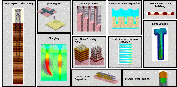
Feature-scale effects, which were once manageable secondary concerns, have moved to the forefront of process control. High-aspect-ratio (HAR) etching, microtrenching, local loading, and ion shadowing now directly dictate the success of a fabrication run. In advanced logic and memory, removing or preserving just a few atomic layers can be the difference between a functional gate and a total device failure. This is particularly evident in Gate-All-Around (GAA) architectures, where the release of nanosheets, the management of residual silicon-germanium (SiGe), and the control of inner spacers must be balanced with extreme precision.
The financial stakes of these technical challenges are reflected in the global equipment market. Industry projections indicate that spending on specialized etch equipment is set to surge from approximately $25 billion today to nearly $40 billion by 2031. This investment underscores the industry’s recognition that more sophisticated hardware is required to meet the demanding requirements of next-generation nodes. However, hardware alone is not the solution; the bottleneck has shifted to the human capacity to explore and optimize the vast innovation space these tools provide.
A Chronology of Process Development: From Trial-and-Error to Virtual Models
To understand the current shift, it is necessary to examine the evolution of process development workflows over the last two decades.
- The Empirical Era (Pre-2010): At larger nodes (above 28nm), process development was largely driven by "design of experiments" (DOE) on physical wafers. Engineers relied on intuition and iterative testing. The number of process "knobs" was relatively limited, allowing for a manageable number of wafer splits to find the optimal recipe.
- The Simulation Integration Era (2010–2020): As FinFET technology emerged at 14nm and 10nm, the three-dimensional nature of the transistors made physical cross-sectioning and empirical testing more difficult and expensive. Technology Computer-Aided Design (TCAD) and feature-scale simulation began to move from academic research into the core of industrial R&D.
- The Digital Twin and AI Era (2021–Present): With the arrival of 3nm and the transition to GAA, the industry has reached a tipping point. The number of possible process interactions has outpaced human reasoning. The current era is defined by the move toward "virtual fabrication," where physics-grounded digital twins allow engineers to run thousands of simulations before a single wafer is processed in a cleanroom.
The Role of Physics-Based Simulation as a Physical Anchor
While AI and machine learning (ML) are frequently cited as the future of manufacturing, industry experts emphasize that these technologies are only as effective as the data they are built upon. In semiconductor manufacturing, where experimental data is expensive and scarce, "pure" AI often fails because it lacks an understanding of the underlying physical laws.
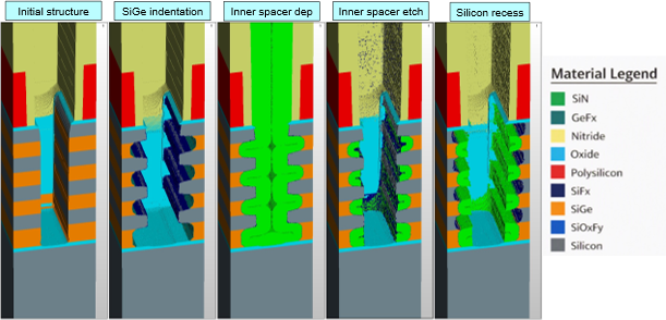
This is where physics-based simulation tools, such as Synopsys Sentaurus Topography, provide a critical differentiator. These tools translate equipment-level inputs—such as power, pressure, and gas chemistry—into feature-level results like profile shape and selectivity. By modeling species transport, surface reaction kinetics, and ion-induced charging, these simulations provide a mechanistic framework that explains why a certain outcome occurs.
For example, in the formation of inner spacers for GAA transistors, the simulation must account for high-aspect-ratio cavity effects and material-dependent selectivity. A physics-based model can predict how neutral species will penetrate a deep trench and how they will react with SiGe versus silicon. This "physical anchor" allows the digital twin to generalize beyond the specific data points of past experiments, enabling it to predict outcomes for entirely new geometries or chemistries that have never been tested in a fab.
Data-Driven Insights: The Economic Necessity of Virtual Exploration
The shift toward simulation is also driven by the staggering costs of modern semiconductor R&D. The cost of a single 3nm wafer run can exceed tens of thousands of dollars, and a full mask set for an advanced node can cost upwards of $15 million. Relying on physical wafers for every iteration is no longer economically viable.
Supporting data suggests that:
- Time-to-Market: Fabs using advanced TCAD and digital twin workflows report a 20% to 30% reduction in the time required to qualify a new process node.
- Yield Ramp: Virtual optimization can identify potential "killer defects" related to profile evolution months before they would be caught in physical testing, significantly accelerating the yield ramp.
- Resource Allocation: By narrowing down thousands of candidate recipes to a handful of high-probability successes, simulation allows process teams to focus their limited "wafer starts" on the most promising innovations.
Automation: Moving from Serial to Parallel Exploration
As simulation capabilities have matured, a new bottleneck has emerged: the time required for expert engineers to set up, calibrate, and interpret these complex models. Creating an accurate surface reaction model is an intensive task that requires translating incomplete fab observations into physically plausible mechanisms.
The industry is now responding with workflow automation. Instead of an engineer manually adjusting parameters in a serial fashion, new "agentic" workflows allow for parallel exploration. In this model, expert knowledge is captured in structured templates. Automation tools then generate multiple candidate mechanisms and run them in parallel across high-performance computing (HPC) clusters.
This does not replace the engineer; rather, it acts as a "force multiplier." The engineer’s role shifts from manual data entry and parameter tweaking to high-level validation and judgment. They are responsible for determining whether the automated outputs are physically credible and which model best aligns with the observed fab data.

The Digital Twin: A Unified Environment for the Fab
The ultimate evolution of this technology is the integrated process digital twin. Unlike a standalone simulation, a digital twin is a living representation of the manufacturing process that incorporates equipment parameters, manufacturing data, and physical models into a single environment.
This platform democratizes simulation. It allows process engineers—not just simulation specialists—to evaluate "what-if" scenarios. An engineer can virtually adjust a pulsed plasma setting or a cryogenic etch temperature and immediately see the predicted impact on the wafer’s profile. This connectivity between virtual predictions and real-world wafer behavior ensures that decision-making is grounded in science rather than trial and error.
Industry Implications and the Path Forward
The integration of physics, AI, and digital twins has profound implications for the global semiconductor supply chain. As the gap between the leaders in advanced node manufacturing and the rest of the industry widens, the ability to effectively use these virtual tools will become a primary competitive advantage. Fabs that can master the "speed of complexity" will be the ones to secure the contracts for the next generation of AI accelerators, high-performance computing chips, and mobile processors.
Furthermore, this shift is changing the talent landscape. The next generation of process engineers will need to be as proficient in data science and simulation as they are in material science and plasma physics. The industry is moving toward a future where the "virtual fab" is just as important as the physical one.
In conclusion, the challenges of semiconductor manufacturing are no longer just about the limits of hardware, but about the limits of human cognition in the face of exponential complexity. By building a foundation of physics-based simulation and layering it with AI and automation, the industry is creating a robust framework for innovation. This synergy ensures that as transistors continue to shrink, the industry’s ability to understand, predict, and control the manufacturing process continues to grow. The future of semiconductor development lies at this intersection, where the laws of physics meet the speed of artificial intelligence to enable the next great leap in technology.
