
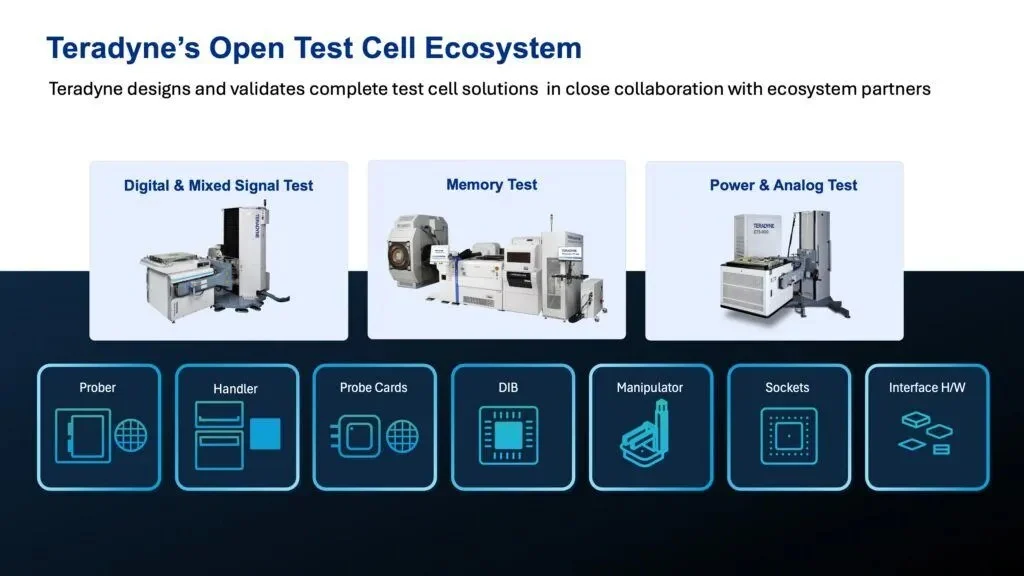

The semiconductor manufacturing landscape is undergoing a fundamental transformation as the industry moves beyond the evaluation of individual machine performance toward a holistic, system-level approach known as the test cell. For decades, the primary metrics for success in semiconductor testing were the raw speed, accuracy, and measurement capabilities of the Automated Test Equipment (ATE). However, as device architectures grow increasingly sophisticated—incorporating chiplets, High-Bandwidth Memory (HBM), and heterogeneous integration—the focus has shifted. Today, the ability to realize optimal throughput, high yield, and superior Overall Equipment Efficiency (OEE) depends on the seamless integration of the entire test cell, a complex ecosystem that serves as the final arbiter of quality before chips are integrated into global supply chains.
The Test Cell as a Unified System Architecture
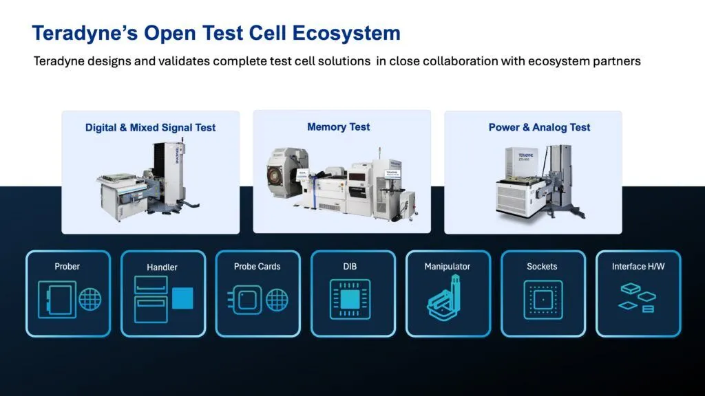
A modern test cell is far more than a collection of disparate tools; it is a tightly integrated system designed for high-volume manufacturing (HVM). At its core, the test cell comprises several critical components: the tester (ATE), the manipulator, the handler or prober, the interface hardware, and application-specific components such as probe cards and load boards. While each of these elements serves a distinct function, their collective performance is dictated by how they interact under rigorous production conditions.
In a high-pressure fab environment, the mechanical alignment between a prober and a tester must be precise to the micron level to ensure electrical continuity. Any minor inefficiency at these interfaces—whether it is a slight misalignment or a microsecond delay in signal synchronization—can lead to false failures or damaged hardware, both of which erode the bottom line. As industry forums like SWTest have highlighted, the challenge is no longer just about making a faster tester; it is about managing the system-level interaction of hardware and software to maintain a stable, repeatable process.
The concept of the test cell also extends to the broader test floor. In large-scale operations, rows of these systems run in parallel, often handling diverse product types simultaneously. To manage this complexity, manufacturers are increasingly turning to automation. This includes autonomous material transport systems (AMRs) that move wafers between stations and programmable manipulators that reduce the need for manual intervention during changeovers. By treating the test cell as a synchronized system architecture, manufacturers can mitigate operator variability and ensure that the test floor operates with the reliability of a high-precision engine.
The Strategic Shift: Complexity Moves Upstream
Historically, the semiconductor test process was bifurcated into two distinct stages: wafer probe (testing the silicon while still in wafer form) and final test (testing the packaged chip). Wafer probe was typically used for basic functional screening, while the more comprehensive validation occurred during the final test. However, the rise of advanced packaging technologies has blurred these boundaries, creating a phenomenon known as "shifting left."
This shift is driven by the move from monolithic designs to heterogeneous integration. In modern AI processors and data center components, logic, memory, and specialized accelerators are combined into a single advanced package. If a single defective chiplet is integrated into an expensive multi-die package, the entire assembly may be rendered useless. To avoid these "scrap" costs, manufacturers are moving more comprehensive testing earlier in the process—specifically to the wafer-level or singulated die level—to ensure that only "Known Good Die" (KGD) proceed to the packaging stage.
This transition introduces significant engineering hurdles. Test cells must now manage higher pin counts, greater power delivery requirements, and tighter alignment tolerances at the wafer level than ever before. Furthermore, new insertion points, such as panel-level testing and sub-assembly testing, require the test cell to be highly adaptable to various form factors and handling requirements.
A Chronology of Test Evolution and Market Context
To understand the current state of the test cell, it is helpful to look at the timeline of its development within the semiconductor industry:
- The 1980s-1990s: Testing was largely manual or semi-automated. Testers were standalone units, and the "cell" concept was loosely defined. The focus was on basic DC measurements and low-speed functional tests.
- The 2000s: The rise of consumer electronics led to the need for higher throughput. Automated handlers became standard, and the industry began to standardize interfaces.
- The 2010s: The mobile revolution demanded massive scale. OEE became a critical metric, and the integration of testers with probers became more sophisticated to handle complex System-on-Chip (SoC) designs.
- 2020-Present: The AI and High-Performance Computing (HPC) boom has pushed testing to its limits. The need for HBM and chiplet testing has made the integrated test cell the industry standard, with a focus on thermal management and "Known Good Die" screening.
Market data underscores the importance of this evolution. The global semiconductor automated test equipment market is projected to grow significantly, driven by the increasing complexity of 5nm, 3nm, and eventually 2nm nodes. As the cost of manufacturing a single wafer climbs into the tens of thousands of dollars, the value of a high-efficiency test cell that prevents defective parts from moving forward becomes an economic necessity.
Engineering Under New Constraints: Footprint and Thermal Management
As test requirements intensify, engineers are facing a new set of physical and operational constraints. One of the most pressing issues is the physical footprint of the test floor. With the demand for semiconductor capacity reaching record highs, fabs are running out of floor space. This has made "throughput per square meter" a vital KPI. Test cell providers are now tasked with designing more compact manipulators and more efficient system layouts that allow for higher density without sacrificing accessibility for maintenance.
Perhaps the most daunting challenge in modern test cell engineering is thermal management. Next-generation AI chips and compute devices generate immense amounts of heat during operation. To accurately test these devices, the test cell must maintain precise temperature control, often requiring active thermal systems that can dissipate hundreds of watts of power from a single chip during the test cycle.
This requires a coordinated dance between the tester and the handler or prober. Real-time feedback loops are used to regulate temperature at the device level, ensuring that the chip is tested under conditions that mimic its eventual operating environment. If the thermal management system fails to keep up, the chip may throttle its performance or sustain permanent damage, leading to inaccurate test results.
The Open Ecosystem: Collaboration as a Catalyst for Success
In response to these multi-domain challenges, the industry is moving away from closed, proprietary models toward an open ecosystem. Teradyne, a leader in the ATE market, has been a vocal proponent of this approach. Rather than attempting to vertically integrate every component of the test cell, the strategy focuses on fostering partnerships with specialized handler, prober, and interface providers.
This ecosystem-based approach allows semiconductor manufacturers to mix and match the best available technologies for their specific needs. For example, a manufacturer focused on AI chips might pair a Teradyne UltraFLEXplus tester with a high-performance prober from Tokyo Electron (TEL).
A recent milestone in this collaborative trend is the partnership between Teradyne and Tokyo Electron. The two companies recently announced an integrated test cell solution designed specifically for AI and data center devices. By integrating Teradyne’s UltraFLEXplus platform with TEL’s Prexa SDP (singulated device prober), they have created a system capable of production-scale Known Good Die testing. This collaboration ensures that the electrical, mechanical, and software interfaces are pre-validated, significantly reducing the time-to-market for chipmakers.
Industry analysts suggest that such collaborations are no longer optional. "As we approach the physical limits of silicon, the ‘easy’ gains in performance are gone," noted one senior industry consultant. "The next frontier of value is in the integration of the manufacturing flow. Companies that can provide a ‘turnkey’ yet flexible test cell environment will win the next decade."
Economic Implications and Future Outlook
The move toward integrated test cells has profound economic implications for the semiconductor industry. Test costs typically represent 5% to 10% of the total manufacturing cost of a device. However, in the era of advanced packaging, the "cost of escape"—the cost of a defective part reaching the customer—can be catastrophic, potentially leading to expensive recalls or the failure of mission-critical systems in automotive or aerospace sectors.
By improving the efficiency and accuracy of the test cell, manufacturers can achieve several key financial objectives:
- Reduced Capital Expenditure (CapEx): Higher throughput per cell means fewer systems are required to meet production targets.
- Improved Yield: Better thermal control and signal integrity reduce the number of "false kills" (good chips marked as bad).
- Faster Time-to-Market: Pre-integrated solutions reduce the months spent on debugging the interface between the tester and the handler.
Looking ahead, the next evolution of the test cell will likely involve the integration of Artificial Intelligence and machine learning. "Smart" test cells will be able to predict hardware failures before they occur, automatically adjust test parameters based on real-time yield data, and communicate with other cells across the globe to optimize production flows.
As the industry gathers at events like SWTest to discuss the future of wafer-level challenges, the consensus is clear: the tester is no longer a standalone tool. It is the heart of a synchronized production system. The companies that will lead the next wave of semiconductor innovation are those that view the test cell not as a collection of parts, but as a strategic asset where engineering capability meets manufacturing reality. In this high-stakes environment, integration is not just a technical preference—it is the defining factor of value.
