

The global push toward electrification, spearheaded by the rapid expansion of the electric vehicle (EV) market and the modernization of industrial power grids, has catalyzed a fundamental shift in semiconductor material science. As traditional silicon reaches its physical limits in high-voltage and high-temperature environments, the industry is pivoting toward wide-bandgap (WBG) materials, specifically silicon carbide (SiC) and gallium nitride (GaN). These materials are no longer niche laboratory curiosities; they are the backbone of the next generation of power electronics, enabling faster charging, longer ranges for EVs, and more efficient renewable energy conversion. However, the transition to these materials, coupled with an aggressive move toward larger wafer diameters, has introduced a suite of manufacturing and inspection challenges that demand a departure from legacy quality-control methodologies.
The Strategic Shift to Wide-Bandgap Power Electronics
The demand for power semiconductors is currently undergoing a structural transformation. Unlike the low-power logic chips found in consumer electronics, power semiconductors must manage high currents and voltages while minimizing energy loss. SiC has emerged as the premier choice for high-voltage applications, particularly in traction inverters that drive EV motors, onboard chargers, and DC-to-DC converters. Its ability to operate at higher temperatures and voltages than silicon allows for smaller, lighter, and more efficient cooling systems within the vehicle.
GaN, conversely, has found its stronghold in high-frequency applications. Its superior electron mobility makes it ideal for fast-charging adapters for consumer electronics and increasingly for the power delivery stages of data centers and telecommunications infrastructure. As these end-markets scale, the semiconductor industry is under immense pressure to increase volume while simultaneously lowering the cost per chip—a feat typically achieved by increasing wafer size.
A Chronological Progression of Wafer Standards
The history of SiC and GaN manufacturing is defined by its substrate transitions. For much of the last decade, 150mm (6-inch) wafers were the industry standard for SiC production. However, to meet the economies of scale required by the automotive industry, the transition to 200mm (8-inch) wafers is currently in full swing. Major industry players, including Wolfspeed, STMicroelectronics, and Onsemi, have invested billions of dollars into 200mm fabrication facilities.
The timeline for these transitions is accelerating. While 150mm was the mainstay until approximately 2020, the shift to 200mm is expected to dominate high-volume manufacturing (HVM) through the mid-2020s. Looking further ahead, research into 300mm (12-inch) SiC substrates has already begun, with early-stage demonstrations occurring in pilot lines. GaN is following a similar trajectory, moving from GaN-on-sapphire or GaN-on-SiC to GaN-on-silicon on 200mm and eventually 300mm platforms.
Each increase in wafer diameter significantly increases the number of available die per wafer, potentially lowering costs by 20% to 30%. However, larger wafers are more prone to mechanical stress, warping, and non-uniformity during the epitaxial growth process, where a thin layer of crystalline material is deposited onto the substrate.
The Complexity of Vertical Device Architecture
A primary factor complicating the inspection of SiC power devices is their vertical architecture. In a standard silicon logic chip, current flows laterally across the surface. In a SiC power MOSFET or diode, the current flows vertically from the front side of the wafer through the substrate to the backside. This design is essential for handling high power densities, but it makes the device exceptionally sensitive to "bulk" or crystalline defects.
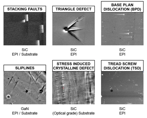
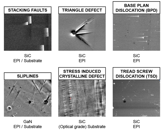
Crystalline defects, such as threading dislocations, basal plane dislocations, and stacking faults, can originate in the initial substrate or be introduced during the epitaxial growth phase. Unlike surface particles, which might only affect a single metal line, a crystalline defect can create a leakage path through the entire thickness of the device. This results in increased resistance, reduced efficiency, or catastrophic dielectric breakdown when the device is subjected to high operational voltages in the field.
Limitations of Conventional Optical Inspection Systems
For decades, the semiconductor industry has relied on optical surface inspection to identify defects. These systems use light scattering and reflection to detect particles, scratches, and pits on the wafer surface. While effective for traditional silicon manufacturing, these techniques have proven insufficient for WBG materials.
The fundamental issue is that many of the most damaging defects in SiC and GaN are subsurface or crystalline in nature. They do not always manifest as a physical protrusion or depression on the surface. Consequently, a wafer may pass a standard optical inspection only to fail during final electrical testing—or worse, fail after it has been integrated into a vehicle’s power module.
Furthermore, the mechanical design of traditional inspection tools is struggling to keep pace with larger wafer sizes. Many legacy systems utilize a "spinning-wafer" architecture. As the wafer spins, a sensor moves from the center to the edge. This creates a disparity in linear velocity and sampling density, leading to a "sensitivity roll-off" where the system is less effective at the wafer’s edge. On a 300mm wafer, this edge-zone represents a significant portion of the total surface area and potential yield.
The Role of Photoluminescence in Defect Intelligence
To address the "blind spots" of optical inspection, manufacturers are increasingly adopting Photoluminescence (PL) inspection. PL is a non-destructive optical technique that involves exciting the semiconductor material with a laser. When the electrons in the material return to their ground state, they emit light (luminescence).
The specific wavelength and intensity of this emitted light are dictated by the material’s crystalline structure. When a crystalline defect is present, it alters the local electronic environment, creating a distinct "signature" in the PL map. This allows manufacturers to visualize stacking faults, dislocations, and even variations in doping concentration that are invisible to the naked eye or standard cameras.
High-sensitivity PL systems, particularly those utilizing XY stage architectures rather than spinning platforms, provide uniform sensitivity across the entire wafer surface. By detecting these defects immediately after epitaxial growth, manufacturers can make "go/no-go" decisions before the wafer undergoes expensive lithography and etching steps.
Integrating Electrical Metrology and Data Analysis
The ultimate goal for power semiconductor manufacturers is "defect intelligence"—the ability to not only see a defect but to predict its impact on the final device. This requires the integration of PL data with non-contact electrical metrology.
One such technique involves corona-charged surface voltage mapping. By applying a non-contact charge to the wafer surface, manufacturers can measure the surface potential and identify regions of high leakage or low breakdown voltage. When this electrical map is overlaid with a PL defect map, a clear picture emerges: the manufacturer can see exactly which crystalline defects are "electrically active" and which are benign.
Industry analysts suggest that this multi-modal approach is critical for "yield learning." By correlating substrate defects with epitaxial defects and final electrical performance, engineers can trace the root cause of failures back to specific steps in the manufacturing process or even to specific substrate suppliers.
Economic Implications and Market Reactions
The economic stakes of SiC and GaN manufacturing are significantly higher than those of traditional silicon. A standard 200mm silicon wafer may cost between $50 and $100. In contrast, a 200mm SiC substrate can cost several thousand dollars due to the slow and energy-intensive crystal growth process (the Physical Vapor Transport method).
Scrapping a SiC wafer at the end of the production line due to a defect that could have been detected at the start represents a massive financial loss. Industry experts estimate that improving yield by just 5% to 10% through advanced inspection can save a high-volume fab tens of millions of dollars annually.
In response to these challenges, equipment manufacturers like Onto Innovation, KLA, and Applied Materials have seen a surge in demand for specialized WBG inspection suites. Automotive OEMs (Original Equipment Manufacturers) are also weighing in, often requiring "known good die" (KGD) certifications that prove every chip in a power module has undergone rigorous subsurface inspection.
Broader Impact and Future Outlook
The transition to an integrated, data-driven inspection strategy is no longer optional for the power semiconductor industry. As the world moves toward a carbon-neutral future, the reliability of the power electronics managing our energy consumption is paramount. A single failure in an EV traction inverter on a highway can have life-threatening consequences, making "zero-defect" manufacturing the target for the automotive supply chain.
The implications of these advancements extend beyond the automotive sector. High-efficiency power conversion is essential for the "green" data centers required to power the current Artificial Intelligence (AI) boom. As AI chips demand more power, the efficiency of the power delivery units (PDUs) becomes a critical bottleneck, one that GaN and SiC are uniquely positioned to solve.
In conclusion, the evolution of power semiconductors is as much a story of metrology and inspection as it is of material science. By moving beyond surface-level detection and embracing technologies like Photoluminescence and integrated electrical mapping, manufacturers are building the foundation for a more reliable, efficient, and electrified global economy. The transition to 200mm and 300mm wafers will continue to push the boundaries of what is possible, but with true defect intelligence, the industry is well-equipped to meet the challenge.
