
The landscape of artificial intelligence for robotics and autonomous vehicles is undergoing a fundamental architectural shift, marked by the rapid ascent of Vision-Language-Action (VLA) models. At the most recent industry gatherings, including the high-profile Embedded Vision Summit, VLAs have moved beyond the realm of academic curiosity to become the primary target for engineering teams developing the next generation of autonomous systems. For silicon architects and system designers, the emergence of VLAs represents both a significant performance hurdle and a transformative opportunity to redefine how machines perceive and interact with the physical world. Unlike traditional modular stacks, VLAs integrate perception, reasoning, and motor control into a single, unified neural network, demanding a new class of hardware capable of handling diverse computational workloads without the bottlenecks associated with legacy heterogeneous architectures.
The Evolution of Autonomous Architectures: From Modular Stacks to VLAs
For decades, robotics and autonomous vehicle systems relied on a "perception-planning-control" stack. In this traditional model, separate software modules handled different tasks: one system processed camera data to detect obstacles, another planned a path through the environment, and a third translated that path into specific motor commands or joint movements. While robust, these modular systems often struggle with "distribution shift"—where a small error in the perception layer cascades into a failure in the control layer—and they generally lack the ability to generalize across different tasks without extensive manual reprogramming.
The VLA model represents an end-to-end alternative. By training a single model on vision, language, and robotic trajectory data simultaneously, developers have created systems that can understand natural language instructions—such as "pick up the red block and place it in the bin"—and translate those directly into physical actions. This shift is largely driven by the success of Large Language Models (LLMs) and Vision Transformers (ViTs). VLAs essentially combine the visual understanding of a ViT with the reasoning capabilities of an LLM and the precision of a motor controller.
Dissecting the Pi-0.5: A Benchmark for Modern VLA Performance
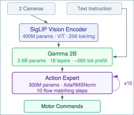
To understand the hardware requirements of this new era, industry experts point to Pi-0.5, a 3.3-billion-parameter open-source VLA recently released by Physical Intelligence. The model serves as a concrete reference point for the industry, as its architecture and weights are publicly available, allowing for rigorous benchmarking across different hardware platforms. The Pi-0.5 operates in three distinct, interconnected stages, each placing unique demands on the underlying silicon.
Stage 1: The Vision Encoder (SigLIP)
The first stage utilizes a SigLIP vision transformer, comprising approximately 400 million parameters. This component processes raw sensor data—typically 16×16-pixel patches from multiple camera feeds—and converts them into 256 "patch tokens" per camera. This stage is characterized by massive compute density, requiring high throughput for matrix multiplications to handle real-time video streams.
Stage 2: The Language Model (Gemma 2B)
The core of the model’s reasoning capability resides in a 2.6-billion-parameter Gemma 2B language model. This decoder-only LLM integrates the vision tokens with natural language instructions and the robot’s current joint positions. Structurally, this is the "prefill" phase of an LLM inference request. It is both compute-intensive and bandwidth-intensive; since 2.6 billion parameters must be loaded from Dynamic Random-Access Memory (DRAM) for every inference, memory bandwidth becomes a critical limiting factor for system responsiveness.
Stage 3: The Action Expert
The final stage is the "Action Expert," a 300-million-parameter transformer decoder. This stage uses a process known as "flow matching" to iteratively refine a noise vector into a sequence of candidate actions. This refinement loop typically runs 10 times per inference. After these iterations, the model outputs approximately 50 action tokens that dictate the robot’s movements for the immediate future.
Crucially, the Action Expert in Pi-0.5 introduces a specific operator called AdaRMSNorm (Adaptive RMS Normalization). This operator conditions normalization parameters based on the specific step of the flow-matching loop. Because AdaRMSNorm is a relatively new addition to the transformer landscape, it is rarely supported by the fixed-function logic found in current Neural Processing Units (NPUs), presenting a significant challenge for hardware deployment.

The Hardware Dilemma: Why Current Solutions Struggle at the Edge
The deployment of VLAs like Pi-0.5 exposes the limitations of existing hardware paradigms, particularly when balancing performance, power consumption, and flexibility.
The Power Wall of Server-Class GPUs
Running a model like Pi-0 on a high-end consumer GPU, such as the NVIDIA RTX 4090, yields a latency of roughly 73 milliseconds. However, this performance comes at the cost of 450 watts of power. While acceptable for a data center or a large laboratory robot, such power draw is untenable for the vast majority of embedded applications. Delivery drones, handheld industrial tools, and sensor modules in production vehicles typically operate within a thermal envelope of 10 to 20 watts.
NVIDIA’s Jetson Thor, designed specifically for autonomous machines, attempts to bridge this gap. It offers approximately 517 INT8 TOPS (Tera Operations Per Second) but still consumes between 120 and 130 watts. For most embedded systems, 130 watts exceeds the total power budget of the entire device, not just the inference processor. Furthermore, roofline analysis suggests that even with extensive optimization, the Jetson Thor would likely achieve an end-to-end latency of 62 to 70 milliseconds, which may still fall short of the requirements for high-speed reactive robotics.
The Heterogeneous NPU Fallback Problem
The most common approach to embedded AI involves a heterogeneous NPU architecture, where a fixed-function accelerator is paired with a legacy CPU or Digital Signal Processor (DSP). The NPU is designed to handle the heavy lifting of matrix multiplications, while the CPU manages any operations the NPU cannot process.
For VLAs, this partitioning creates a severe performance bottleneck. Every transformer layer in a VLA combines "MAC-heavy" (Multiply-Accumulate) operations with "non-MAC" operations like softmax, layer normalization, and the aforementioned AdaRMSNorm. In a typical heterogeneous setup, every time the model encounters an unsupported operator, the task must be handed off (or "fallen back") to the CPU.
Research into on-device LLM inference has shown that in such architectures, the NPU can remain idle for up to 37% of the time due to the overhead of these CPU fallbacks. For a model like Pi-0.5, this partitioning can generate over 700 round-trips between the NPU and CPU per inference, adding hundreds of megabytes of extra memory transfers. This overhead is compounded by the 10 iterations required by the Action Expert’s flow-matching loop, leading to high latency and excessive power consumption.
The GPNPU Alternative: Programmability and Performance
In response to these challenges, a new category of processor has emerged: the General-Purpose Neural Processing Unit (GPNPU). Quadric’s Chimera GPNPU is a leading example of this shift toward fully programmable AI acceleration. Unlike fixed-function NPUs, a GPNPU uses a single processor pipeline containing an array of processing elements (PEs), each equipped with its own 32-bit scalar ALU and local memory.
By utilizing a software-controlled architecture, GPNPUs can execute the entire operator graph of a VLA natively. There is no need for a fallback processor, which eliminates the latency and power penalties associated with data shuffling between disparate cores.
Direct Mapping and Weight Tiling
On a Chimera core, the vision encoder’s patch tokens can be mapped directly to the PE array, allowing data to stay in place throughout the attention block. For the language model stage, where weights are too large for on-chip SRAM, software-managed weight tiling allows the system to prefetch the next set of weights via Direct Memory Access (DMA) while the current tile is being processed. This hides memory latency behind computation, a feat that is difficult to achieve with the non-deterministic caching mechanisms of traditional CPUs.

Native Execution of Custom Operators
The most significant advantage of the GPNPU approach is its ability to handle evolving model architectures. Because the PEs are fully programmable, new operators like AdaRMSNorm can be implemented in software and run on the same array used for matrix multiplications. This ensures that the hardware remains relevant even as researchers release new VLA variants with different normalization or attention mechanisms.
Comparative Data and Industry Benchmarks
When comparing performance across platforms, the GPNPU demonstrates a clear advantage in efficiency. Simulated data for a configuration of eight Chimera QC-U cores running the 3.3-billion-parameter Pi-0.5 model shows an end-to-end latency of approximately 45 milliseconds. This is notably faster than the 53-millisecond theoretical "roofline" limit of the Jetson Thor for the smaller 3-billion-parameter Pi-0 model.
Even more striking is the power efficiency. The Chimera GPNPU cores consume approximately 11 watts, compared to the 120-130 watts of the Jetson Thor. Even when accounting for DDR memory interfaces and other SoC elements—which might bring the total chip power to 20 or 25 watts—the GPNPU offers a 5x to 10x improvement in performance-per-watt over high-end GPU-based edge solutions.
| Metric | RTX 4090 | Jetson Thor | Chimera GPNPU (8x QC-U) |
|---|---|---|---|
| Model | Pi-0 (3B) | Pi-0 (3B) | Pi-0.5 (3.3B) |
| INT8 TOPS | ~1,300 | ~517 | 445 |
| Memory Bandwidth | 1,008 GB/s | 273 GB/s | 273 GB/s |
| Power Consumption | 450W | 120-130W | ~11W (cores) |
| E2E Latency | 73 ms (measured) | ~53 ms (roofline) | ~45 ms (simulated) |
Broader Impact and the Future of Silicon Design
The rapid evolution of VLA models carries profound implications for the semiconductor industry and the future of autonomous systems. The "silicon re-spin" cycle—where a chip is designed for a specific set of AI operators only to be rendered obsolete by a new model release a year later—is no longer sustainable. The complexity of VLAs suggests that the industry must move toward more flexible, programmable architectures that can adapt to software innovations through compilation rather than hardware redesign.
Industry analysts suggest that the success of future autonomous systems will depend less on raw TOPS and more on "effective utilization"—the ability of a processor to keep its compute units busy across the entire neural network graph. As VLAs continue to integrate more modalities and more complex reasoning loops, the bottleneck will increasingly be the interface between different processor types.
For companies developing delivery robots, autonomous drones, or advanced driver-assistance systems (ADAS), the choice of AI processor is now a strategic long-term decision. Systems that rely on fixed-function NPUs risk being locked into outdated model architectures, while those adopting programmable GPNPU solutions may find themselves better positioned to integrate the rapid breakthroughs coming out of AI research labs.
In conclusion, the rise of Vision-Language-Action models marks a turning point in robotics. By unifying perception and action, VLAs offer a path toward truly intelligent, general-purpose machines. However, realizing this potential at the edge requires a departure from traditional hardware design. The shift toward programmable, high-efficiency acceleration is not just a performance upgrade; it is a necessary evolution to meet the demands of the most sophisticated AI models ever built for the physical world.
