
Taiwan Semiconductor Manufacturing Co. (TSMC), the world’s leading dedicated semiconductor foundry, recently utilized its annual North America Technology Symposium to announce a significantly expanded and aggressive technology roadmap. This strategic update introduces three new advanced process nodes—A13, A12, and N2U—while detailing the company’s progress in backside power delivery, advanced packaging, and silicon photonics. As the industry grapples with the immense computational demands of generative artificial intelligence (AI) and high-performance computing (HPC), TSMC’s latest roadmap underscores a pivot toward optimizing area efficiency, power consumption, and signal latency. The announcement serves as a clear signal to both competitors and customers that the foundry is accelerating its transition into the angstrom era, moving beyond the traditional constraints of FinFET architecture into more sophisticated nanosheet and backside power delivery systems.

Strategic Evolution of the TSMC Advanced Technology Roadmap
The updated roadmap represents a notable shift from the projections shared at the 2025 symposium. By introducing A13 and A12 into the 2029 timeframe and N2U into 2028, TSMC is effectively filling gaps in its performance tiers to provide chip designers with more granular choices for power-performance-area (PPA) optimization. The roadmap is now clearly bifurcated between the established N2 (2-nanometer) family and the emerging A-series (angstrom-class) nodes.
Currently, the N2 process is in the early stages of production. TSMC leadership confirmed that customer adoption for N2 has been the strongest in the company’s history, surpassing the initial ramp-up phases of both the N3 and N5 nodes. To date, more than 20 customer tape-outs have been received, with an additional 70 designs currently in the pipeline. This momentum is bolstered by the fact that N2 is ramping with a defect density reduction rate that is faster than that of its predecessor, N3. This is particularly significant because N2 represents TSMC’s first departure from FinFET (Fin Field-Effect Transistor) toward NanoFlex nanosheet transistor structures, a transition that usually involves a steep learning curve in manufacturing yield.

Deep Dive into the Angstrom Era: A16, A14, A13, and A12
The "A" prefix in TSMC’s new nomenclature refers to the angstrom scale, marking the next generation of silicon scaling. The transition is not merely a marketing rebrand but a fundamental shift in how power is delivered to the transistors.
The A16 node, previously advertised for a late 2026 production start, has been adjusted in the latest roadmap to a 2027 launch. A16 will be the first TSMC node to integrate Super Power Rail (SPR) technology. SPR is a backside power delivery system that moves the power distribution network from the front of the wafer to the back. This innovation addresses the "IR drop" (voltage drop) and routing congestion issues that have plagued sub-3nm designs, allowing for more efficient power delivery and freeing up the front-side metal layers for signal routing.

Building on this, the A14 node is slated for 2028, utilizing an enhanced NanoFlex Pro technology. NanoFlex allows designers to mix and match different standard cell heights within a single block, optimizing for either high speed or high density.
The two newest additions, A13 and A12, are scheduled for 2029. A13 is described as a direct "shrink" of the A14 node, promising a 6% savings in silicon area. Crucially for design houses, the design rules for A13 are fully backward compatible with A14, significantly reducing the engineering overhead required to migrate designs to the newer node. Meanwhile, A12 is positioned as a performance-enhanced version of the A14 platform that incorporates the SPR backside power technology. The introduction of A12 for 2029 is viewed by industry analysts as an aggressive acceleration of TSMC’s angstrom-class deployment, intended to maintain a competitive lead over rivals like Intel and Samsung.

N2U and the Refinement of 2nm Technology
While the angstrom nodes represent the long-term future, TSMC is also refining its current 2nm portfolio. The newly announced N2U (N2-Ultra) node is scheduled for production in 2028. N2U serves as an incremental improvement over the N2P node.
The N2U enhancement is designed to offer a balanced improvement across the PPA spectrum. By providing a bridge between the initial 2nm designs and the more radical angstrom architectures, N2U allows customers who are not yet ready to move to backside power delivery to still achieve performance gains through refined nanosheet transistor tuning and improved metal pitch scaling.

Advanced Packaging: The Rise of CoWoS and System-on-Wafer
As Moore’s Law slows in terms of traditional monolithic scaling, TSMC is increasingly relying on advanced packaging to drive system-level performance. The demand for AI compute scaling has made Chip-on-Wafer-on-Substrate (CoWoS) technology a critical bottleneck and a primary revenue driver.
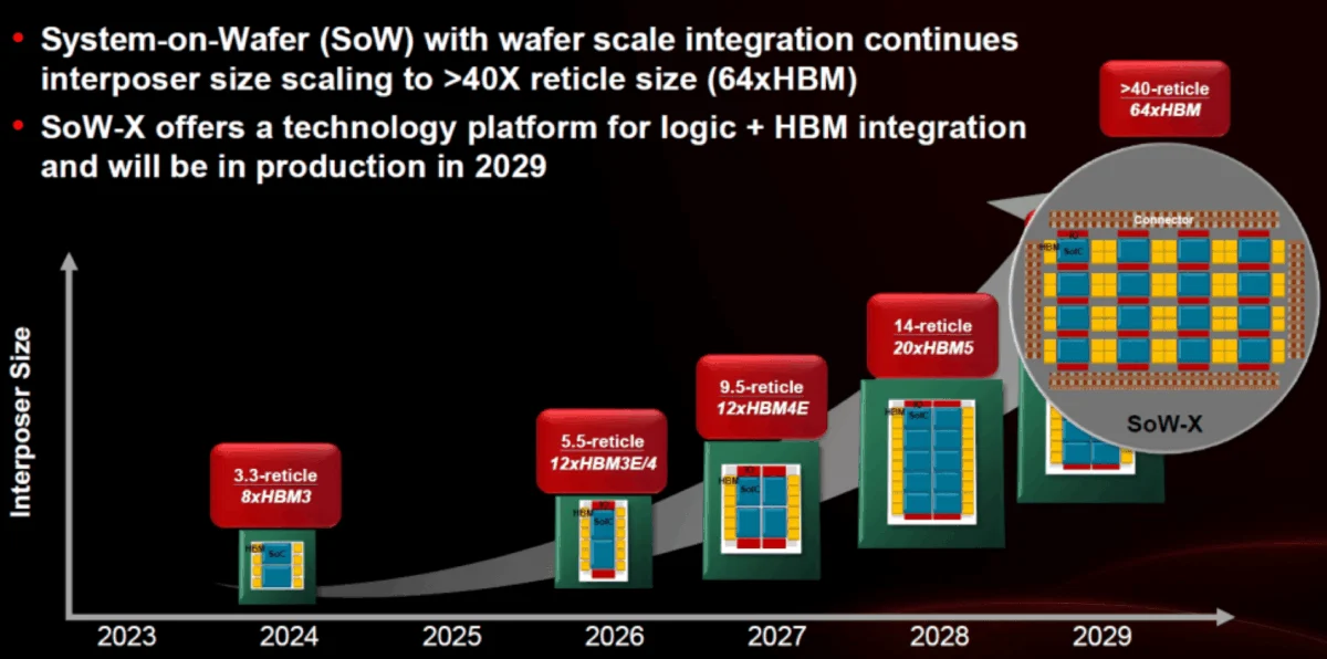
TSMC announced that it is currently manufacturing the world’s largest CoWoS solutions, reaching 5.5-reticle sizes. Despite the complexity of these massive interposers, the company claims a yield of over 98% for 2026 production. Looking toward 2029, TSMC’s roadmap for System-on-Wafer (SoW) integration envisions the SoW-X platform. This technology is projected to accommodate up to 64 High Bandwidth Memory (HBM) stacks. Given the industry’s trajectory toward 64GB HBM stacks by 2029, this implies a staggering 4 terabytes (TB) of HBM integrated on a single SoW-X system. Such a development would revolutionize the training of large language models (LLMs), which are currently limited by memory capacity and data transfer speeds between discrete chips.

Silicon Photonics and the COUPE Engine
Data movement remains one of the greatest energy consumers in modern data centers. To address this, TSMC is advancing its co-packaged optics (CPO) solutions through its Compact Universal Photonics Engine (COUPE).
The COUPE roadmap shows a progression toward bringing optical signaling closer to the processor die. By integrating silicon photonics directly with the logic and memory through advanced 3D stacking, TSMC aims to reduce latency and improve energy efficiency by several orders of magnitude compared to traditional copper-based interconnects. As AI clusters grow to include tens of thousands of GPUs, the transition to optical interconnects facilitated by COUPE will be essential to prevent the "interconnect bottleneck" from stalling compute progress.

Financial Context and Market Displacement
The technical roadmap is supported by a robust financial performance that reflects a changing semiconductor landscape. In its first-quarter 2026 earnings call, TSMC reported a dramatic shift in its revenue mix. For the first time in the company’s history, the High-Performance Computing (HPC) and AI segments have decisively displaced smartphones as the primary revenue generator.
Historical data shows that while smartphone revenue remained dominant for over a decade, the surge in AI infrastructure investment has fundamentally altered the foundry’s priorities. Revenue from advanced nodes (N7, N5, and N3) has remained remarkably consistent over the last six quarters, providing a stable financial foundation for the massive R&D expenditures required for A16 and beyond. As N2 begins to contribute to the bottom line, analysts expect the revenue share from sub-5nm technologies to exceed 60% of TSMC’s total wafer revenue by the end of 2027.

Industry Implications and Competitive Landscape
TSMC’s aggressive roadmap is a direct response to a revitalized competitive environment. Intel, under its "five nodes in four years" strategy, has been vocal about reclaiming process leadership with its Intel 18A node. Similarly, Samsung Foundry has been pushing its Gate-All-Around (GAA) technology aggressively to win back market share in the mobile and AI sectors.
By announcing A13 and A12, TSMC is attempting to close any perceived windows of opportunity for its competitors. The focus on backward compatibility (as seen in A13) and the rapid deployment of backside power (SPR) are designed to keep the world’s most valuable chip designers—including Apple, Nvidia, and AMD—locked into the TSMC ecosystem.

Furthermore, the emphasis on yield and defect density is a subtle jab at competitors who have struggled with manufacturing consistency at the leading edge. TSMC’s ability to ramp N2 more efficiently than N3 suggests that the company has mastered the complexities of nanosheet manufacturing, a prerequisite for the angstrom-class nodes that follow.
Conclusion: A Multi-Front Strategy for the Future
The 2026 North America Technology Symposium has clarified TSMC’s vision for the remainder of the decade. The strategy is multi-faceted: continue scaling through nanosheet transistors (N2 to A14), innovate in power delivery (SPR), lead the industry in advanced packaging (CoWoS/SoW), and solve the data movement challenge with silicon photonics (COUPE).

For the broader technology industry, TSMC’s roadmap provides a predictable, albeit aggressive, schedule for the next generation of hardware. As AI continues to evolve from niche research into the backbone of the global economy, the silicon foundation provided by TSMC’s A-series and N2 families will be the primary engine driving that transformation. The focus on area savings, power efficiency, and reduced latency ensures that the "AI era" will have the necessary hardware substrate to sustain its current exponential growth through 2030 and beyond.
