
A collaborative research initiative involving scientists from Utsunomiya University, RIKEN, The University of Tokyo, and Tohoku University has achieved a significant milestone in semiconductor manufacturing technology by demonstrating a 40% increase in the conversion efficiency (CE) of extreme ultraviolet (EUV) light. By utilizing simultaneous dual-beam irradiation from a 2-µm Holmium-doped Yttrium Aluminum Garnet (Ho:YAG) laser on a planar tin (Sn) target, the team has established a new benchmark for energy-efficient EUV generation. This development is poised to address one of the most critical bottlenecks in the scaling of next-generation lithography: the requirement for high-power, sustainable light sources to support the production of sub-2nm logic and memory chips.
The research, published in June 2026, details how splitting a single laser pulse into two identical beams—maintaining the same total energy but optimizing the interaction with the target material—resulted in a jump from 2.6% to 3.6% conversion efficiency. While these percentages may appear small to the layperson, in the context of high-volume manufacturing (HVM), a 1% absolute increase representing a 40% relative boost is a transformative gain. This efficiency gain allows for higher throughput in lithography scanners while reducing the immense thermal load and energy consumption associated with current EUV source technologies.
The Evolution of EUV Lithography and the Search for Efficiency
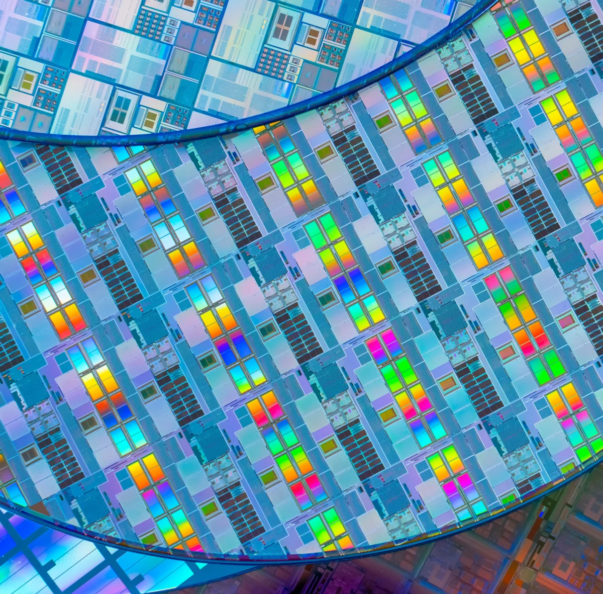
To understand the magnitude of this breakthrough, it is necessary to examine the current state of semiconductor fabrication. Extreme ultraviolet lithography, which operates at a wavelength of 13.5 nanometers, is the foundational technology used by foundries like TSMC, Samsung, and Intel to print the microscopic features of modern microprocessors. The light is generated by hitting microscopic droplets of molten tin with high-powered lasers, creating a plasma that emits EUV radiation.
Historically, the industry has relied on carbon dioxide (CO2) lasers operating at a wavelength of 10.6 µm. While effective, these systems are notoriously inefficient and require massive amounts of electricity to produce the kilowatts of EUV power needed for modern scanners. As the industry moves toward High-NA (Numerical Aperture) and eventually Hyper-NA lithography, the demand for EUV power is expected to double or triple. Increasing the conversion efficiency—the ratio of EUV energy produced to the laser energy consumed—is the only viable path to making these future nodes economically and environmentally sustainable.
The shift toward 2-µm wavelength lasers, such as the Ho:YAG laser used in this study, represents a strategic pivot in plasma physics research. Shorter wavelengths compared to CO2 lasers offer a more favorable interaction with the tin plasma, potentially allowing for smaller source sizes and higher brightness, which are essential for the tighter focus required by High-NA optics.
Experimental Methodology and Data Analysis
The research team, led by Naoki Nagahama and Eiji J. Takahashi, focused their experiments on a planar tin target to isolate the variables of laser-plasma interaction. The primary objective was to compare the efficiency of a single-beam configuration against a dual-beam configuration while keeping the total energy delivered to the target constant.
In the baseline experiment, a single 2090-nm laser pulse with an energy of 40 mJ was fired at the tin target. This setup yielded an EUV conversion efficiency of 2.6%. The researchers then modified the optical path to split the 40 mJ pulse into two separate 20 mJ beams. These beams were directed to strike the target simultaneously at the same peak intensity. Despite the total energy remaining at 40 mJ, the dual-beam configuration produced a 3.6% conversion efficiency.
Several key metrics were monitored to ensure that the quality of the light source was not compromised by the dual-beam approach:
- Source Size: The EUV source size remained consistent between 60 and 70 µm in both configurations. This is critical because a larger source size would negate the efficiency gains by making it harder for the scanner’s collector mirrors to capture and focus the light.
- Ion Spectra: The energetic-ion spectra—a measure of the particles ejected from the plasma—were nearly identical across both setups. This confirms that the dual-beam approach does not increase the risk of "debris" or ion damage to the expensive multilayer mirrors used in EUV scanners.
- Wavelength Stability: The emission remained centered at the required 13.5 nm band, ensuring compatibility with existing reflective optics.
The researchers attribute this 40% boost to the optimized spatial distribution of the laser energy. By using two beams, the plasma expansion is better controlled, and a larger volume of the tin target reaches the optimal temperature for EUV emission without wasting energy on over-heating a single focal point.

Chronology of Development in EUV Source Technology
The journey to this 40% efficiency boost is the result of decades of incremental progress in laser-produced plasma (LPP) research.
- 2000s: Early research focused on Nd:YAG lasers (1.06 µm). However, these were found to be less efficient than CO2 lasers for EUV generation because the plasma produced was too dense, causing the EUV light to be re-absorbed before it could escape the plasma cloud.
- 2010s: The industry standardized on CO2 lasers (10.6 µm). By using a "pre-pulse" technique—where a small laser pulse hits a tin droplet to flatten it into a pancake shape before a main pulse hits it—efficiencies reached the 3% to 5% range in laboratory settings, though lower in production environments.
- Early 2020s: Limitations of CO2 lasers, including their massive footprint and high cooling requirements, led researchers back to solid-state lasers. The 2-µm wavelength emerged as a "sweet spot" that combines the benefits of shorter wavelengths with better plasma penetration.
- 2024-2025: Research into Ho:YAG lasers gained momentum due to their high pulse repetition rates and potential for scaling.
- June 2026: The publication of the dual-beam 2-µm study by the Japanese consortium provides a practical roadmap for exceeding the efficiency limits of current CO2-based systems.
Implications for High-NA and Hyper-NA Lithography
The semiconductor industry is currently transitioning to High-NA EUV lithography, which uses a numerical aperture of 0.55 compared to the 0.33 of standard EUV machines. These machines, spearheaded by ASML, allow for higher resolution but suffer from significant light loss due to the complex mirror configurations. Consequently, the light source must be much more powerful to maintain the same wafer-per-hour throughput.
The dual-beam 2-µm scheme offers several strategic advantages for the High-NA era:
- Throughput Scalability: A 40% increase in CE directly translates to more wafers processed per hour for the same electricity cost. In a multi-billion dollar fabrication plant (fab), this can be the difference between a profitable and a non-profitable node.
- Passive Scalability: One of the most promising aspects of the research is that the scheme requires only passive beam splitting. This means it can be integrated into existing laser architectures without requiring a fundamental redesign of the laser engine itself. The researchers noted that the system could potentially scale to three or more beams for even greater gains.
- Thermal Management: By distributing the laser energy more efficiently, the thermal stress on the tin delivery system and the vacuum chamber is reduced, potentially extending the lifespan of the source components and reducing downtime for maintenance.
Institutional Collaboration and Official Perspectives
The success of this research is a testament to the collaborative ecosystem in Japan, involving top-tier academic institutions and national research centers. The involvement of Utsunomiya University and RIKEN highlights a bridge between theoretical plasma physics and industrial application.
While official statements from commercial equipment manufacturers like ASML or Gigaphoton regarding this specific paper are pending, the industry has long signaled that "multi-beam" and "short-wavelength" solid-state lasers are the future of the EUV roadmap. Analysts suggest that the transition from CO2 to 2-µm solid-state lasers could be the most significant change in lithography hardware since the introduction of EUV itself.
The research team concluded that their findings offer a "practical route toward multi-kW-class, energy-efficient EUV sources." By demonstrating that comparable plasma conditions can be maintained while significantly boosting light output, the team has removed a major hurdle for the "Hyper-NA" generation of chips, which will likely target features below 10 angstroms.
Future Outlook: Beyond Dual-Beam Systems
Looking forward, the research team plans to explore the effects of multi-beam irradiation on spherical tin droplets, which are used in actual industrial scanners, as opposed to the planar targets used in this study. The transition from a flat target to a droplet presents challenges in beam alignment and timing, but the underlying physics of the 2-µm interaction remains the same.
Furthermore, the integration of artificial intelligence and real-time feedback loops to adjust the intensity and timing of the dual beams could push the conversion efficiency even higher. If the industry can reach a 5% or 6% CE using 2-µm lasers, the power constraints that currently limit the speed of the world’s most advanced chip factories could be permanently alleviated.
As the demand for artificial intelligence chips and high-performance computing continues to surge, the ability to print more transistors on a single slice of silicon depends entirely on the efficiency of the light used to etch them. The 40% boost achieved by Nagahama, Takahashi, and their colleagues marks a vital step toward a future of sustainable, ultra-high-resolution semiconductor manufacturing.
