
The challenge of determining when a design is truly "ready" involves a multidimensional assessment of Power, Performance, and Area (PPA) targets, alongside a rigorous verification of logical and structural integrity. Suresh Barla, senior director of field applications at Synopsys, recently highlighted that the sheer volume of variables—ranging from clock domain crossings to the management of thousands of design waivers—has transformed sign-off from a checklist into a sophisticated data-management exercise. As designs scale to include dozens of specialized blocks and heterogeneous components, the industry is seeing a shift toward more automated, AI-driven methodologies to ensure that no critical flaw is buried beneath the noise of massive datasets.
The Evolution of Sign-off Complexity
Historically, chip sign-off was a relatively straightforward process focused on timing closure and basic functional verification. However, the timeline of semiconductor evolution over the last decade has fundamentally altered this landscape. In the early 2010s, as the industry moved through the 28nm and 16nm nodes, the primary concerns were largely centered on thermal design power (TDP) and basic signal integrity. Today, at the leading edge, designers must account for a plethora of "new" physics, including electromigration, IR drop, and complex multi-patterning requirements at the lithography level.
The chronology of this complexity can be traced through the rise of FinFET transistors and the more recent transition to Gate-All-Around (GAA) architectures. Each architectural shift introduces more parasitic elements that must be modeled accurately during the RTL-to-GDSII flow. According to industry data, the cost of a failed "tape-out"—the final handoff to the foundry—can now exceed $30 million to $100 million for advanced nodes when including the cost of lost market opportunity and mask set re-spins. Consequently, the definition of "readiness" has shifted from "mostly functional" to "mathematically verified under all possible corners."
RTL Optimization and the Quest for PPA
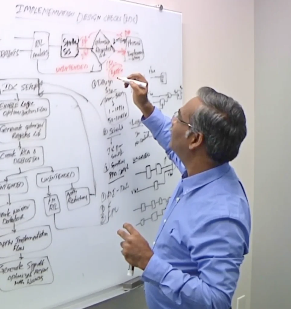
At the core of the sign-off challenge is the optimization of the RTL. This is the stage where the architectural intent of the chip is translated into hardware description language. Suresh Barla notes that for large designs, ensuring the RTL is fully optimized for PPA targets is no longer a manual task. If the RTL is inefficient, no amount of downstream physical synthesis can fully recover the lost performance or power efficiency.
Optimization today requires a "shift-left" approach, where sign-off quality analysis is performed earlier in the design cycle. This involves:

- Area Reduction: Pruning redundant logic and optimizing gate-level implementation to fit within strict die-size constraints.
- Power Analysis: Implementing sophisticated clock-gating and power-gating strategies to meet the stringent energy envelopes required by mobile and data center applications.
- Performance Tuning: Identifying critical paths early to ensure the design can hit target gigahertz frequencies without violating thermal limits.
Supporting data from EDA (Electronic Design Automation) leaders suggests that designs utilizing early-stage RTL optimization see a 10% to 15% improvement in final PPA metrics compared to those that rely solely on back-end physical optimization. This early visibility is crucial for managing the "hundreds of millions of gates" that Barla identifies as the current standard for high-performance computing (HPC) and AI chips.
The Verification Bottleneck and the Role of Waivers
Perhaps the most significant obstacle to sign-off is the verification bottleneck. As designs become more complex, the number of warnings and errors generated by static analysis tools increases. In a design with 500 million gates, a standard linting or Clock Domain Crossing (CDC) check might produce tens of thousands of violations.
The process of "waivers"—where an engineer manually reviews a violation and determines it is not a threat to the design—has become a significant point of risk. If an engineer incorrectly waives a legitimate bug, the resulting silicon could be non-functional. Conversely, if the team spends too much time investigating "noise" or false positives, the product will miss its market window.
Barla emphasizes that the goal is to generate a netlist that meets "sign-off quality," which means the verification tools must be precise enough to distinguish between structural requirements and ignorable artifacts of the design process. This requires a robust methodology for Reset Domain Crossing (RDC) and formal verification, ensuring that even in the most complex asynchronous designs, data integrity is maintained across different power and clock domains.
Industry Responses and Strategic Shifts
The semiconductor ecosystem has responded to these challenges through increased collaboration between EDA providers and foundries. Synopsys, Cadence, and Siemens EDA have all integrated machine learning (ML) algorithms into their sign-off tools. These ML layers are designed to recognize patterns in design violations, automatically suggesting waivers for known non-issues and highlighting high-risk areas that require human intervention.
Industry analysts suggest that the move toward "Digital Twins" and virtual prototyping is also gaining traction. By creating a software representation of the hardware long before the first silicon is poured, companies can run billions of cycles of verification code. This helps in confirming that the RTL is not just optimized for PPA, but is also robust against the diverse software workloads it will eventually run.

In statements regarding the current state of the industry, executives have noted that "the era of ‘good enough’ verification is over." There is an emerging consensus that as we approach the physical limits of silicon, the margin for error in sign-off is narrowing toward zero. This has led to a surge in demand for senior field applications directors and verification architects who can navigate the interface between high-level architectural intent and low-level physical constraints.
Broader Implications for the Global Economy
The ability to successfully sign off on complex chips has implications far beyond the engineering lab. The global economy is increasingly dependent on the timely delivery of advanced semiconductors for everything from automotive safety systems to generative AI infrastructure. A delay in a flagship chip design can impact the quarterly earnings of global tech giants and disrupt supply chains for consumer electronics.
Furthermore, the complexity of sign-off is driving a consolidation of expertise. Only a handful of companies globally possess the tooling, intellectual property (IP), and human capital required to bring a 3nm design to manufacturing. This creates a high barrier to entry, reinforcing the dominance of established players while simultaneously pushing the industry toward "chiplets" and modular architectures. By breaking a massive design into smaller, more manageable blocks or chiplets, companies hope to reduce the individual sign-off risk of each component, even if the systemic complexity of the final package increases.
Conclusion: The Path Forward
As Suresh Barla and other experts in the field continue to refine the methodologies for RTL optimization and netlist verification, the definition of "ready to ship" will continue to evolve. It is no longer enough for a design to pass a set of static tests; it must be resilient, efficient, and manufacturable at scale.
The future of chip design sign-off lies in the integration of deeper analytics and the continued "shifting left" of quality checks. By identifying PPA bottlenecks and verification hurdles at the RTL stage, rather than at the final netlist stage, engineering teams can ensure that when they finally do sign off, the transition to manufacturing is a formality rather than a gamble. In the high-stakes world of semiconductor manufacturing, the difference between a market-leading product and a multi-million-dollar failure often comes down to the rigor of these final verification steps. The industry’s ongoing investment in more sophisticated EDA tools and automated workflows remains the primary defense against the mounting tide of design complexity.
