
The challenge, as identified by industry experts including David Shin, senior product marketing manager at Cadence Design Systems, stems from a fundamental disconnect between the high-voltage requirements of legacy USB specifications and the low-voltage tolerance of modern FinFET and Gate-All-Around (GAA) transistors. While USB remains the most ubiquitous interface in computing history, the roadmap for integrating its various versions requires a deep understanding of physical layer (PHY) dynamics, power management, and signal integrity.
The Physical Voltage Gap: Why USB 2.0 and eUSB2 Diverge
To understand the current integration roadmap, one must first examine the electrical disparity between standard USB 2.0 and the embedded variant, eUSB2. The original USB 2.0 specification, which has remained a staple of digital connectivity for over two decades, operates on a 3.3V signaling voltage. This was easily managed in older process nodes (such as 65nm or 40nm), where the gate oxide of the transistors was thick enough to handle such high voltages without degradation.
However, as the industry pushed toward "Advanced Nodes" (sub-7nm), the physical properties of the silicon changed. Modern transistors utilize extremely thin gate oxides to achieve high-speed switching and power efficiency. These thin oxides cannot withstand 3.3V; they are typically designed to operate at 1.0V or 1.2V. If an engineer were to apply 3.3V directly to a 3nm chip, the resulting electrical stress would cause immediate and permanent damage to the circuitry.
This created a paradox: how can a cutting-edge smartphone or AI processor, built on a 5nm process, communicate with a standard USB 2.0 peripheral? The solution was the creation of the eUSB2 (embedded USB2) Physical Layer Supplement. Unlike the standard USB 2.0 PHY, the eUSB2 PHY operates at a much lower signaling voltage—typically 1.0V or 1.2V. This allows the USB interface to be integrated directly into advanced SoCs without the need for bulky, high-voltage I/O rings that consume excessive die area and power.
Chronology of USB Evolution and the Rise of eUSB
The roadmap for these standards is best understood through the timeline of their development and the market pressures that drove their adoption:

- 2000 – The USB 2.0 Era Begins: USB 2.0 is released, offering "High Speed" data rates of 480 Mbps. It becomes the global standard for almost all consumer electronics, utilizing 3.3V signaling.
- 2008-2013 – The Transition to SuperSpeed: USB 3.0 and 3.1 are introduced. While they offer much higher speeds (5-10 Gbps), they maintain backward compatibility with USB 2.0. This means every USB 3.x port still needs to support the 3.3V USB 2.0 signaling.
- 2014-2015 – The Advanced Node Crisis: As mobile processors move to 16nm and 14nm FinFET processes, the area required for 3.3V I/O starts to become disproportionately large compared to the shrinking logic cores.
- 2018 – The eUSB2 Specification: The USB Implementers Forum (USB-IF) releases the eUSB2 specification. This allows internal chip-to-chip communication and internal-to-external port communication to happen at 1.0V/1.2V.
- 2020-Present – The Integration Era: Designers begin implementing eUSB2 in mass-market SoCs. The focus shifts from "how to make it work" to "how to make it compatible" with the billions of 3.3V USB devices already in existence.
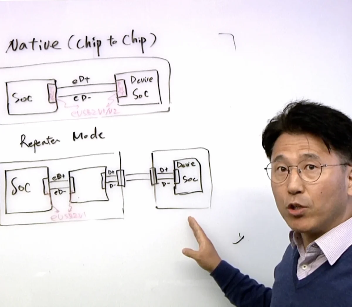
Technical Mechanisms of Integration: The Role of the Repeater
A primary point of confusion in the integration roadmap is how an eUSB2-based SoC connects to a traditional USB-C or USB-A port. Because the eUSB2 signal is electrically incompatible with the 3.3V USB 2.0 signal, a "bridge" or "repeater" is required.
In a typical modern design, the SoC contains an eUSB2 PHY. This PHY sends a low-voltage (1.0V) signal across the PCB to a small, inexpensive component called an eUSB2-to-USB 2.0 repeater. This repeater acts as a translator: it takes the 1.0V signal and "boosts" it to 3.3V for the external world. Conversely, when an external 3.3V device is plugged in, the repeater steps the voltage down to 1.0V before it reaches the sensitive SoC.
This architecture offers three distinct advantages:
- Area Efficiency: The SoC no longer needs to dedicate massive amounts of space to high-voltage I/O transistors.
- Power Savings: Low-voltage signaling consumes significantly less power, which is critical for battery-operated devices like smartphones and wearables.
- Signal Integrity: By moving the high-voltage transition closer to the physical port, the SoC remains protected from the noise and electrical interference associated with 3.3V signaling.
Supporting Data: The Impact on Die Area and Power
Data from semiconductor design firms highlights the necessity of this transition. In a standard 7nm SoC, a traditional USB 2.0 PHY capable of 3.3V signaling can take up to five times more area than an eUSB2 PHY. Furthermore, the power consumption of the I/O alone can be reduced by as much as 80% when switching from 3.3V to 1.0V signaling for internal data paths.
According to Cadence Design Systems, the integration of eUSB2 is not merely an option but a requirement for any design utilizing nodes below 7nm. The "confusion" mentioned by David Shin often arises during the validation phase. Engineers must ensure that the "link layer"—the part of the chip that manages data packets—can communicate seamlessly across the "physical layer" (the eUSB2 PHY) and through the external repeater without introducing latency or protocol errors.
Expert Analysis: Why Standards Conflict
The central irony of the USB roadmap is that the drive for universality has created a fragmented ecosystem of internal and external specifications. David Shin points out that the difficulty in controlling these versions stems from the diverse needs of the market. A high-end server chip might prioritize raw speed (USB4), while a micro-controller for a smart thermostat might prioritize low power and cost (eUSB2).

"Just because it’s a standard doesn’t mean everything will work together," Shin notes. This is particularly true in the "handshake" phase of a USB connection. When a device is plugged in, the host and the peripheral must agree on speed and voltage. If the eUSB2 repeater is not perfectly synchronized with the SoC’s link layer, the handshake fails, and the device defaults to the slowest possible speed or fails to connect entirely. This necessitates rigorous simulation and verification using high-quality Intellectual Property (IP) blocks.
Broader Implications for Edge AI and Chiplets
The roadmap for USB and eUSB integration extends beyond simple consumer gadgets. It has profound implications for the burgeoning fields of Edge AI and chiplet-based architectures.
Edge AI and Power Constraints:
As AI models move to the "edge" (local devices like cameras and sensors), the power budget for data transfer becomes miniscule. Edge AI chips must process vast amounts of data while remaining thermally efficient. The power savings provided by eUSB2 are vital in these applications, allowing for constant data streaming from sensors to the AI processor without draining the battery or requiring active cooling.
The Chiplet Revolution:
The industry is moving toward a "chiplet" model, where a single package contains multiple smaller chips (die) instead of one giant monolithic chip. In this environment, internal connectivity is king. eUSB2 provides a standardized, low-power method for these chiplets to communicate with one another within the same package. The integration roadmap must now account for "die-to-die" communication, where the distances are measured in micrometers rather than centimeters on a PCB.
Conclusion: Navigating the Roadmap
The integration of USB and eUSB standards represents a microcosm of the challenges facing the semiconductor industry at large. It is a story of the relentless pursuit of Moore’s Law crashing into the reality of legacy compatibility. For design teams, the roadmap is clear but demanding:
- Adopt eUSB2 for Advanced Nodes: Stop attempting to force 3.3V I/O into sub-7nm designs.
- Utilize High-Quality Repeaters: Ensure the bridge between the internal low-voltage world and the external high-voltage world is robust and validated.
- Focus on Verification: Use sophisticated EDA (Electronic Design Automation) tools to simulate the entire signal path, from the SoC link layer through the eUSB2 PHY to the external connector.
As we look toward the future of USB4 and beyond, the role of eUSB will only grow. The complexity of these "conflicting" standards is the price of progress—a necessary hurdle to clear in the quest for smaller, faster, and more efficient electronic devices. The roadmap is no longer a straight line; it is a sophisticated multi-layered architecture that requires precision, foresight, and a deep respect for the laws of physics at the nanometer scale.
